

Impedance matching apparatus
a technology of impedance matching and apparatus, which is applied in the field of impedance matching apparatus, can solve the problems of insufficient matching accuracy of the matching circuit according to the cited document, inability to disregard the impedance matching performance of the impedance component, and the inability to match the impedance component with sufficient accuracy
- Summary
- Abstract
- Description
- Claims
- Application Information
AI Technical Summary
Benefits of technology
Problems solved by technology
Method used
Image

Examples
first embodiment
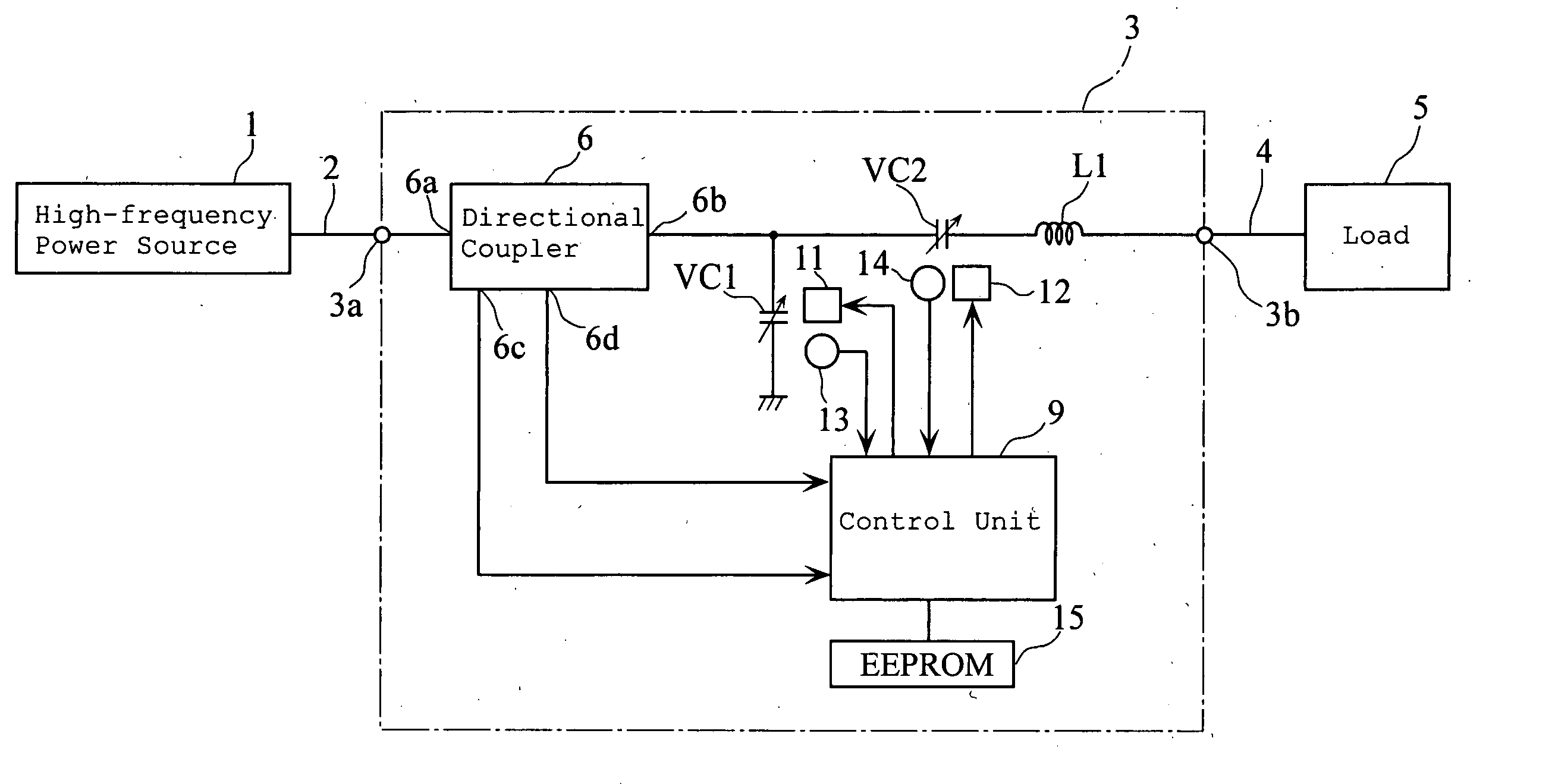
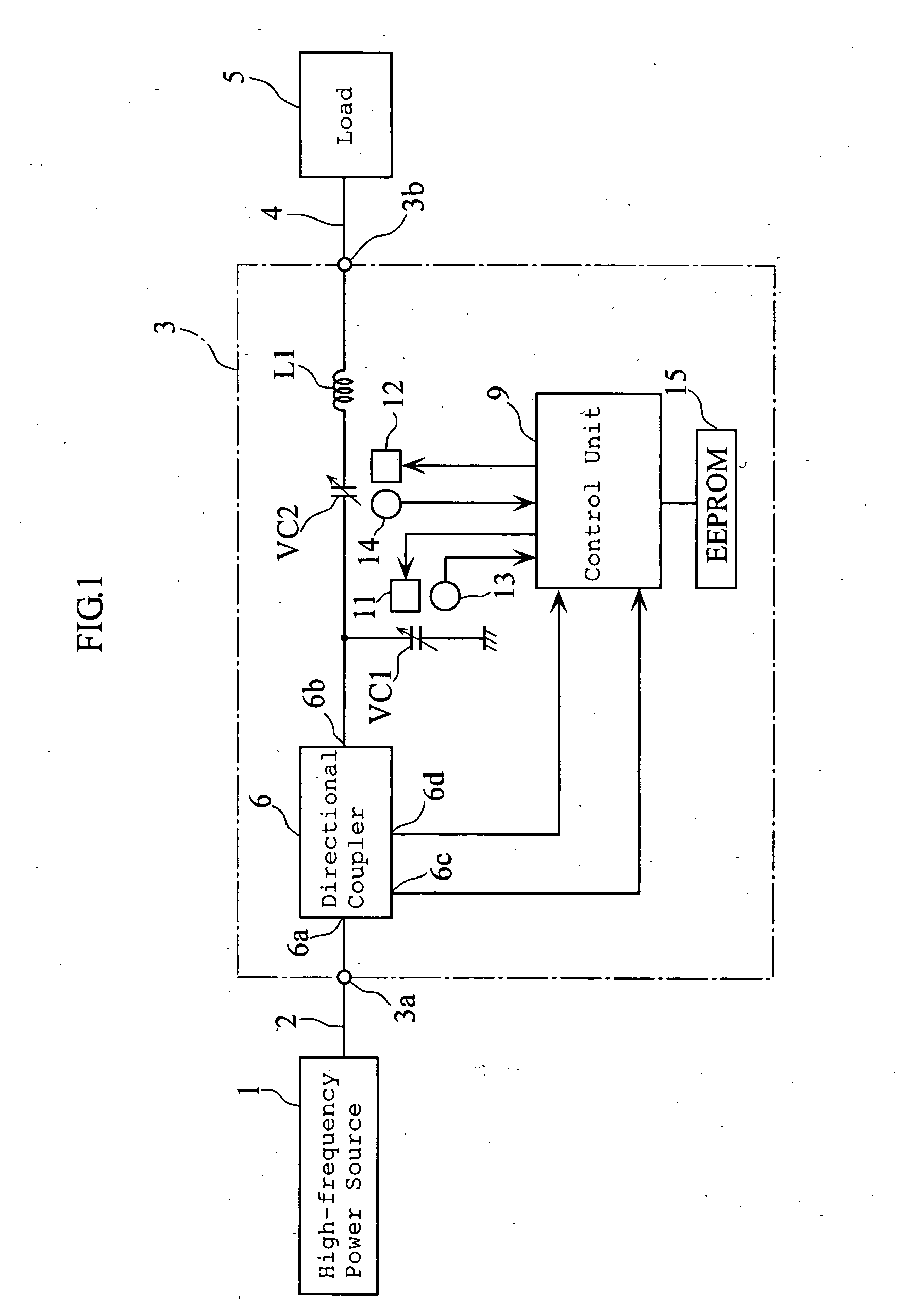
[0036]FIG. 1 is a block diagram showing a configuration of a high-frequency power supply system including an impedance matching apparatus according to the present invention, and a circuit diagram of the impedance matching apparatus.
[0037] The high-frequency power supply system supplies a high-frequency wave to an object to be processed such as a semiconductor wafer or a liquid crystal substrate, to thereby perform a processing such as plasma etching. The high-frequency power supply system includes a high-frequency power source 1, a transmission line 2, an impedance matching apparatus 3, a load connector 4 and a load 5 including a plasma processing apparatus (plasma process chamber).
[0038] The high-frequency power source 1 supplies a high-frequency power with a predetermined frequency (for instance, 13.56 MHz or 200 MHz) to the load 5. The high-frequency power source 1 is connected to the impedance matching apparatus 3 via the transmission line 2, which is for example a coaxial cabl...
second embodiment
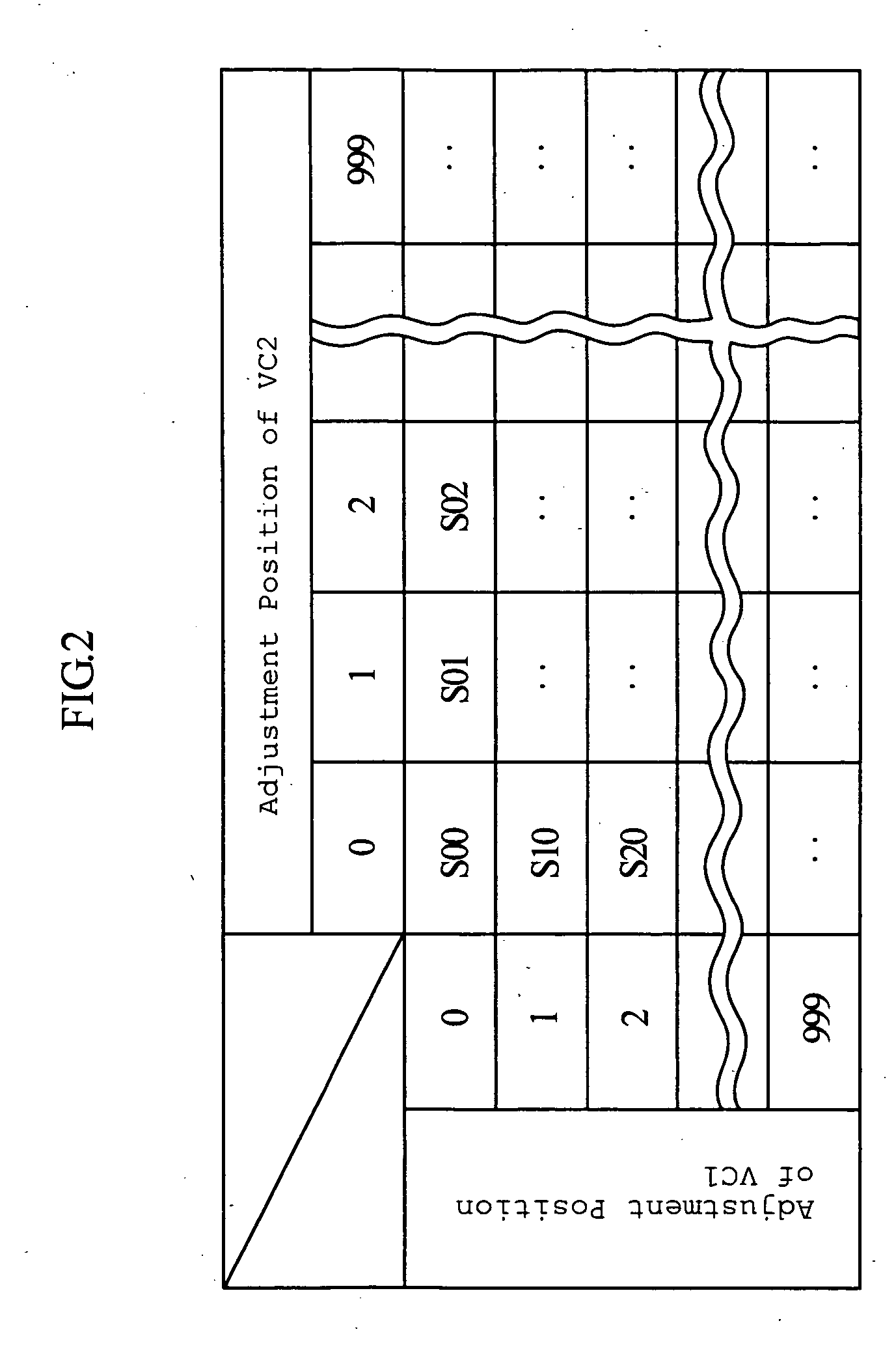
[0130] As described above, the impedance matching apparatus 3 is utilized as a transmission apparatus as a whole, so as to acquire the transmission characteristic of the transmission apparatus in a form of the information on the S parameter and the T parameter with respect to the adjustable range of the variable capacitors VC1, VC2, to thereby perform the impedance matching based on such information. Such method allows performing the impedance matching with higher accuracy in comparison with the conventional impedance matching method.
[0131] Also, since the target input reflection coefficient Γ′ is preset, the virtual output reflection coefficient calculator 32 only has to calculate once the virtual output reflection coefficient Γo′ corresponding to all the combinations of the adjustment positions of the variable capacitors VC1, VC2, unless the target input reflection coefficient Γ′ has to be modified after activating the system. The control unit 9 according to the first embodiment ...
PUM
 Abstract
Description
Claims
Application Information