
Focusing apparatus and lithography system using the same

a focusing apparatus and lithography technology, applied in the direction of photomechanical equipment, magnetic discharge control, instruments, etc., can solve the problems of conventional electron beam lithography system, inconvenient ebl system, and inability to complete one pattern at a time,

Inactive Publication Date: 2006-07-13
SAMSUNG ELECTRONICS CO LTD
View PDF10 Cites 4 Cited by
  • Summary
  • Abstract
  • Description
  • Claims
  • Application Information

AI Technical Summary

Benefits of technology

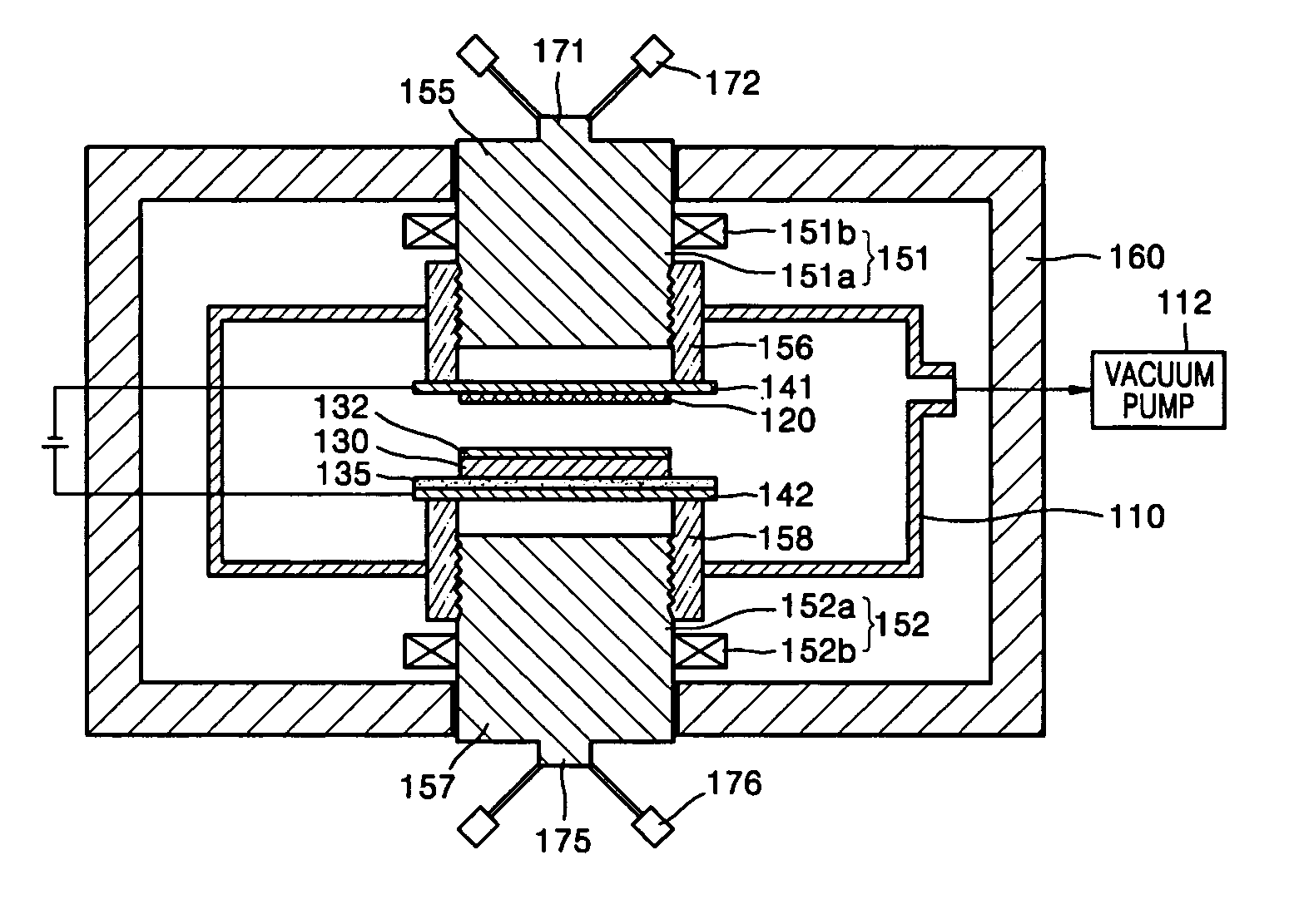
[0016] Example embodiment of the present invention may provide a focusing apparatus and a lithography system using the same, and more particularly, to a focusing apparatus and a lithography system using the same, which can adjust a uniformity of an electromagnetic field.
[0017] Example embodiment of the present invention may provide an electromagnetic focusing apparatus and an electron-beam lithography system using the same, and more particularly, to an electromagnetic focusing apparatus and an electron-beam lithography system using the same, which can adjust a uniformity of an electromagnetic field.
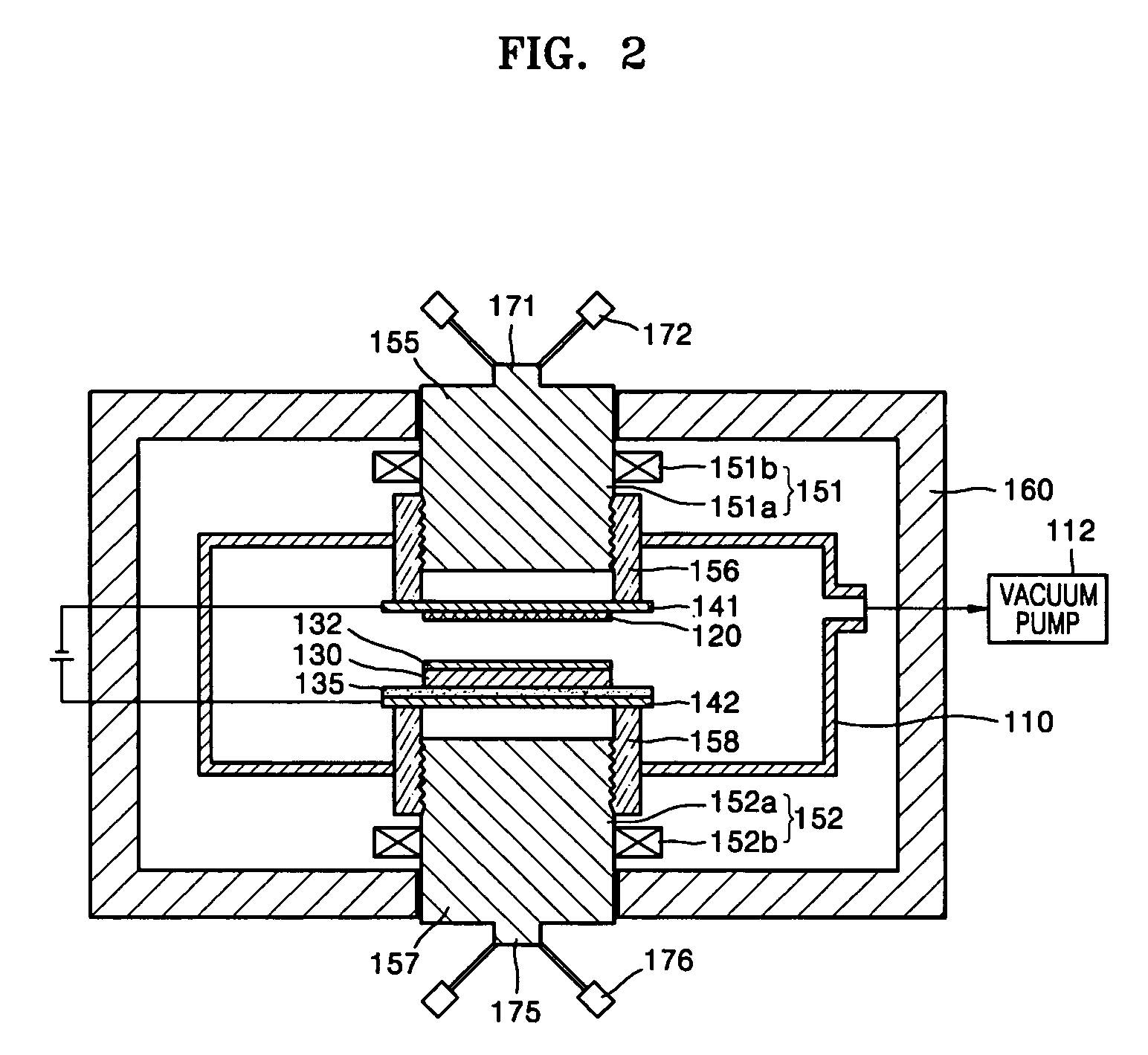
[0028] Example embodiment of the present invention may provide a focusing apparatus and a lithography system using the same, and more particularly, to a focusing apparatus and a lithography system using the same, which can adjust a uniformity of an electromagnetic field by moving a center position of a pole piece.
[0029] Example embodiment of the present invention may provide an electromagnetic focusing apparatus and an electron-beam lithography system using the same, and more particularly, to an electromagnetic focusing apparatus and an electron-beam lithography system using the same, which can adjust a uniformity of an electromagnetic field by moving a center position of a pole piece.
[0030] Example embodiments of the present invention may provide an electromagnetic focusing apparatus and an electron-beam lithography system using the same, which can compensate for a wafer size change due to a temperature change in a vacuum chamber by adjusting a uniformity of an electromagnetic field through the movement of a center position of a pole piece.
[0031] Example embodiments of the present invention may also provide an electromagnetic focusing apparatus and an electron-beam lithography system using the same, which can reduce the space of the system and the manufacturing cost of a large magnet.

Problems solved by technology

However, optical lithography techniques may have a limitation with regard to a possible linewidth.
Accordingly, a conventional EBL system may undesirably require a lot of time to complete one pattern.
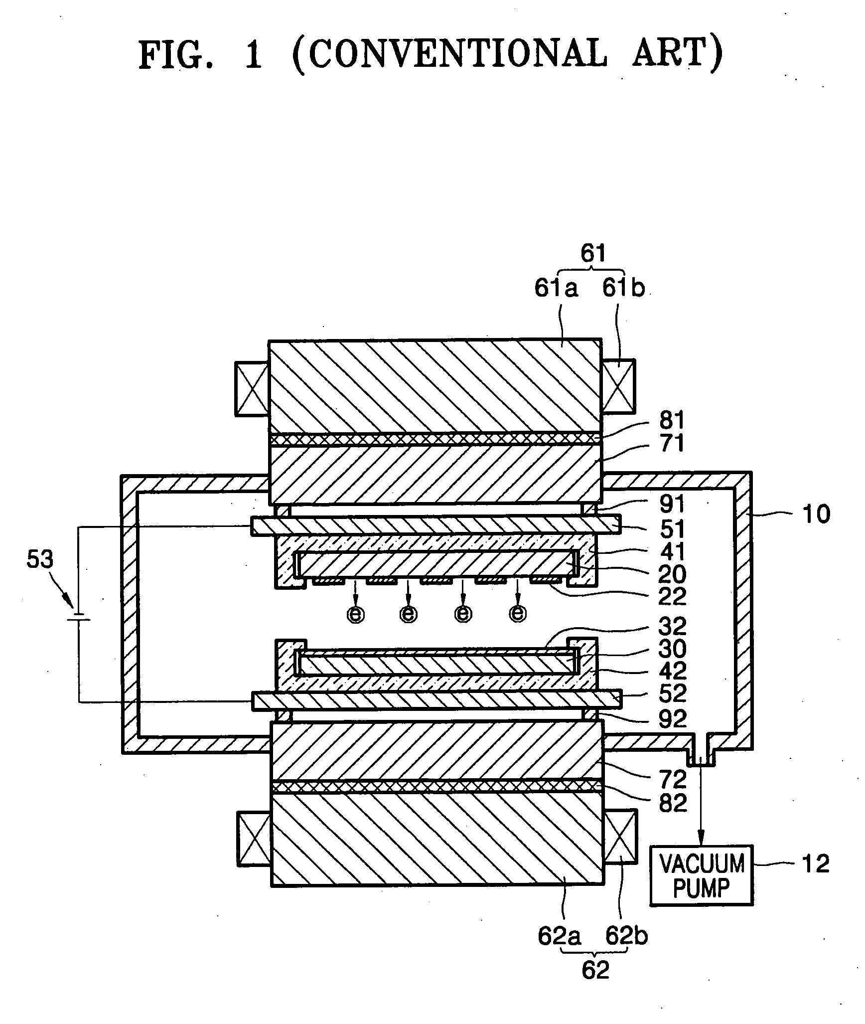
However, a conventional electron-beam lithography system, such as the one illustrated in FIG. 1 cannot suitably compensate for a size change of the wafer 30 resulting from a temperature change, because the positions of the upper and lower pole pieces 71 and 72 are fixed.
Such a size change may cause a problem when a linewidth of several ten nanometers needs to be realized via a semiconductor manufacturing process.

Method used


Image

  • Focusing apparatus and lithography system using the same
  • Focusing apparatus and lithography system using the same
  • Focusing apparatus and lithography system using the same

Examples


Embodiment Construction

[0046] Example embodiments of the present invention will now be described more fully with reference to the accompanying drawings, in which example embodiments of the invention are shown.

[0047] The present invention will now be described more fully with reference to the accompanying drawings, in which example embodiments of the invention are shown. The invention may, however, be embodied in many different forms and should not be construed as being limited to the example embodiments set forth herein; rather, these example embodiments are provided so that this disclosure will be thorough and complete, and will fully convey the concept of the invention to those skilled in the art. Like reference numerals in the drawings denote like elements.

[0048] Example illustrative embodiments of the present invention are disclosed herein. However, specific structural and functional details disclosed herein are merely representative for purposes of describing example embodiments of the present inve...


PUM


Abstract

A focusing apparatus and a lithography system using the same capable of adjusting a uniformity of an electromagnetic field by moving a portion of a magnetic field generator. The focusing apparatus may control a path of an electron beam generated from an electron-beam emitter of the lithography system. In the focusing apparatus, a uniformity of the magnetic field in the vacuum chamber may be adjusted through movement of the portion of the magnetic field generator with respect to the vacuum chamber.

Description

PRIORITY STATEMENT [0001] This application claims the benefit of Korean Patent Application No. 10-2004-0109269, filed on Dec. 21, 2004, in the Korean Intellectual Property Office, the disclosure of which is incorporated herein in its entirety by reference. BACKGROUND OF THE INVENTION [0002] 1. Field of the Invention [0003] Example embodiments of the present invention relate to a focusing apparatus and a lithography system using the same, and more particularly, to a focusing apparatus and a lithography system using the same, which can adjust a uniformity of an electromagnetic field. [0004] 2. Description of the Related Art [0005] Various lithography techniques may be used for patterning a surface of a substrate into a desired pattern in a semiconductor manufacturing process. An optical lithography technique may be used for surface patterning. However, optical lithography techniques may have a limitation with regard to a possible linewidth. Accordingly, a next generation lithography (...

Claims


Application Information

Patent Timeline
Patent Type & Authority Applications(United States)
IPC IPC(8): H01J1/50
CPCB82Y10/00B82Y40/00H01J3/22H01J37/067H01J37/145H01J37/304H01J37/3174H01J2237/31776H01J2237/31777H01J2237/31781G03F7/2051G03F7/70383
Inventor MOON, CHANG-WOOKKIM, DONG-SOOSONG, MYUNG-GONLEE, SEUNG-WOONOH, YUN-SANG
Owner SAMSUNG ELECTRONICS CO LTD
Learn More