Semiconductor integrated circuit and fabrication process thereof

a technology of silicon substrate and integrated circuit, which is applied in the direction of semiconductor devices, basic electric elements, electrical equipment, etc., can solve the problems of leakage current flowing between the source and drain region of silicon substrate, and achieve the effects of suppressing leakage current, suppressing cvd oxide film erosion, and increasing the thickness of sidewall insulation film

Active Publication Date: 2006-07-13
FUJITSU LTD
View PDF2 Cites 57 Cited by
  • Summary
  • Abstract
  • Description
  • Claims
  • Application Information

AI Technical Summary

Benefits of technology

[0069] According to the present invention, a large uniaxial stress is induced in the channel region of the p-channel MOS transistor by forming the p-type SiGe mixed crystal regions so as to fill the trenches at both lateral sides of the channel region and such that the p-type SiGe mixed crystal regions are located closely to the channel region. At the same time, the present invention secures a sufficient distance, in the n-channel MOS transistor formed on the same silicon substrate, between the deep source and drain diffusion regions formed in the silicon substrate. Thereby, it becomes possible to suppress the leakage current between the source region and the drain region of the n-channel MOS transistor effectively.
[0071] It should be noted that the present invention solves the foregoing problem by using a material resistant to HF for the sidewall insulation film of the gate electrode of the p-channel MOS transistor and at the same time suppresses the leakage current by securing a large distance, in the silicon substrate, between the deep source and drain regions in the n-channel MOS transistor, by increasing the thickness of the sidewall insulation film of the gate electrode.
[0072] Further, the present invention can suppress the erosion of the CVD oxide film covering the surface of the first and second gate electrodes by HF, by forming each of the first and second sidewall insulation films in the form of lamination of: the lower sidewall insulation film resistant to HF; the intermediate sidewall insulation film formed on the lower sidewall insulation film and not resistant to HF; and the upper sidewall insulation film formed on the intermediate sidewall insulation film with resistance to HF. Thereby, the electrical properties of the semiconductor integrated circuit device is improved significantly.
[0073] Particularly, it is desirable with the present invention to interpose a film experiencing etching by HF, such as a CVD oxide film, between the gate electrode and the HF-resistant sidewall film and between the HF-resistance sidewall insulation film and the silicon substrate, for improvement of the interface characteristics. Thereby, the present invention avoids the problem of such a film not resistant to HF being etched by the cleaning processing conducted by HF at the time of forming the trenches, by forming the HF-resistant sidewall insulation film on the gate electrode via the film not resistant to HF, and then processing the structure thus obtained with an HF etchant to remove a part of the foregoing film not resistant to HF at the top surface of the gate electrode and at the sidewall surface of the sidewall insulation film. Thereby, a slit structure is formed in correspondence to such a part. Further, the present invention fills such a slit with a film resistant to HF. With the structure thus obtained, no such a slit is formed anymore even when an HF treatment is conducted later at the time of formation of the trenches.

Problems solved by technology

However, various problems are encountered when attempt is made to form the p-channel MOS transistor with an n-channel MOS transistor simultaneously on the same substrate.
On the other hand, when the thickness of the sidewall insulation film of the gate electrode is decreased in the n-channel MOS transistor in the same manner, the source region of n-type and the drain region of n-type are disposed too closely to each other in the device region, and there arises a problem that leakage current is caused to flow between the source and drain regions in the silicon substrate.

Method used


Image

  • Semiconductor integrated circuit and fabrication process thereof
  • Semiconductor integrated circuit and fabrication process thereof
  • Semiconductor integrated circuit and fabrication process thereof

Examples


first embodiment

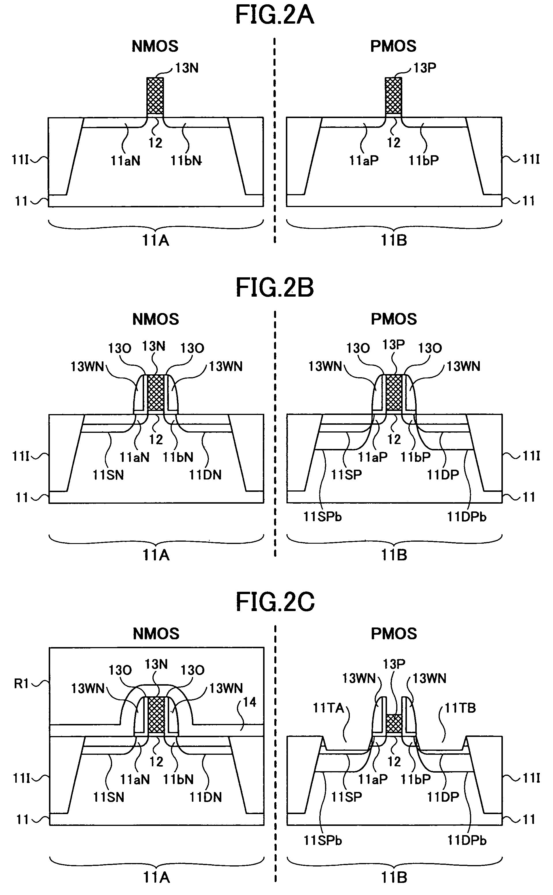
[0087]FIGS. 2A-2F are diagrams showing the fabrication process of a semiconductor integrated circuit device according to a first embodiment of the present invention.

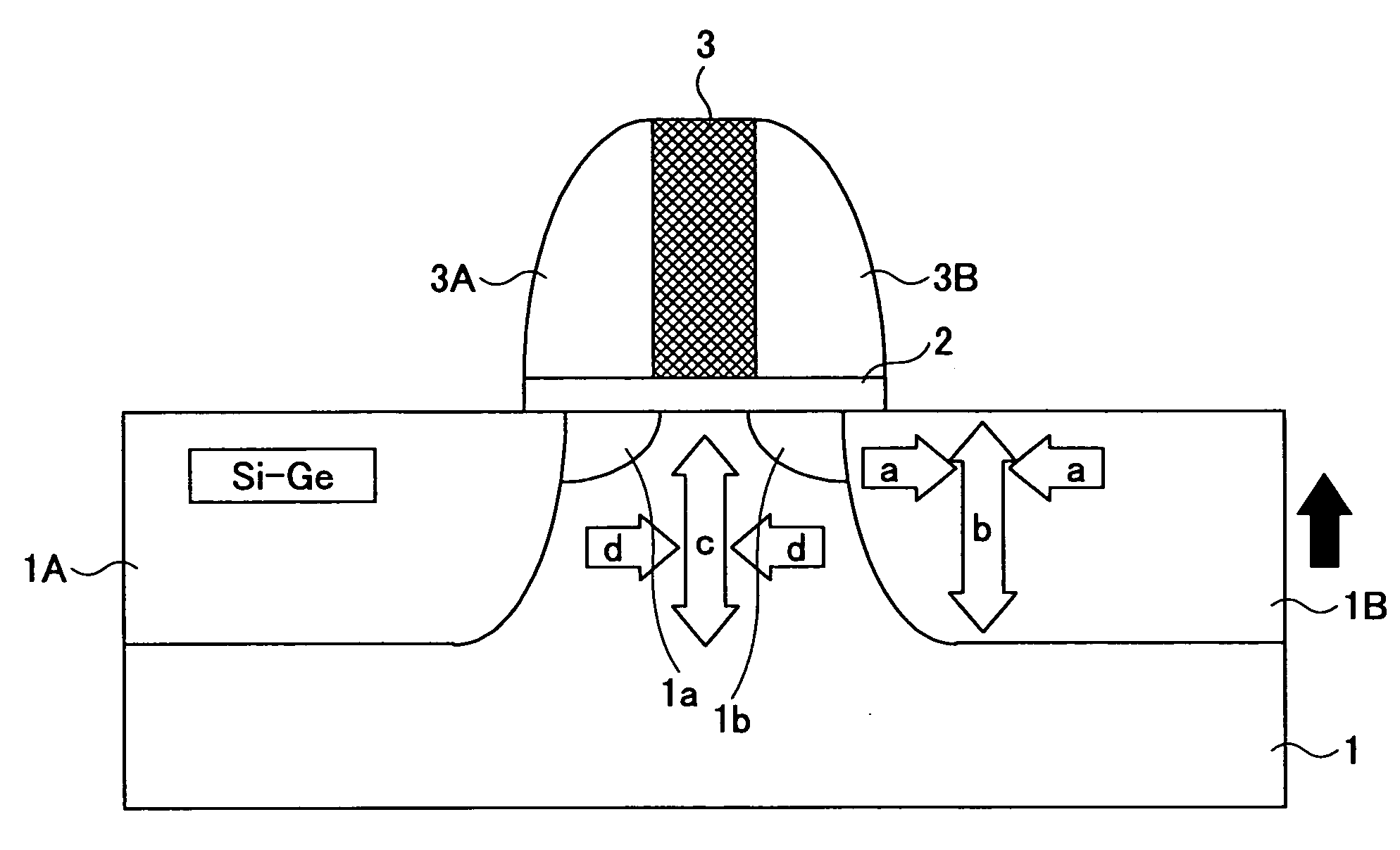
[0088] Referring to FIG. 2A, a silicon substrate 11 is defined with a device region 11A for an n-channel MOS transistor and a device region 11B for a p-channel MOS transistor by an STI device isolation structure 11I, wherein the device region 11A is doped to p-type and forms a p-type well while the device region 11B is doped to n-type and forms an n-type well. Further, while not illustrated, there is conducted an ion implantation of a p-type impurity element in the device region 11A at a surface part of the silicon substrate 11 for the purpose of threshold control of the n-channel MOS transistor. Similarly, there is conducted an ion implantation of an n-type impurity element in the device region 11B at a surface part of the silicon substrate 11 for the purpose of threshold control of the p-channel MOS transistor.

[0089]...

second embodiment

[0114] Next, fabrication process according to a second embodiment of the present invention will be described with reference to FIGS. 4A-4F, wherein those parts corresponding to the parts described previously are designated by the same reference numerals and the description thereof will be omitted.

[0115] Referring to FIGS. 4A-4F, the process of FIGS. 4A and 4B are identical with the process of FIGS. 2A and 2B, and thus, the description thereof will be omitted.

[0116] In the present embodiment, the outside sidewall oxide films 14W are formed at the outer sides of the sidewall insulation films 13WN with the thickness of about 40 nm in the process of FIG. 4C by the deposition and etch back of the CVD oxide film in both of the device regions 11A and 11B, and in this state, the foregoing n−-type buffer source and drain diffusion regions 11DNb and 11DNb are formed by conducting an ion implantation process of an n-type impurity element into the silicon substrate 11 in the device region 11A...

third embodiment

[0122] Next, the fabrication process of the semiconductor integrated circuit according to a third embodiment of the present invention will be explained with reference to FIG. 5A-5F, wherein those parts corresponds to the parts explained previously are designated by the same reference numerals and the explanation thereof will be omitted.

[0123] Referring to FIG. 5A-5F, the process of FIG. 5A is identical to the process of FIG. 2A or FIG. 4A explained previously and the explanation thereof will be omitted.

[0124] In the process of FIG. 5B, the SiN sidewall insulation films 13WN are formed on the respective sidewall surfaces of the polysilicon gate electrodes 13N and 13P similarly to the process of FIG. 4B, except that no further ion implantation process is conducted in the step of FIG. 5B in the present embodiment and the process proceeds to the step of FIG. 5C.

[0125] In the step of FIG. 5C, the outer sidewall oxide films 14W are formed at respective outer sides of the SiN or SiON si...


PUM


Abstract

A semiconductor integrated circuit device includes an n-channel MOS transistor formed on a first device region of a silicon substrate and a p-channel MOS transistor formed on a second device region of the silicon substrate, wherein the n-channel MOS transistor includes a first gate electrode carrying a pair of first sidewall insulation films formed on respective sidewall surfaces thereof, the p-channel MOS transistor includes a second gate electrode carrying a pair of second sidewall insulation films formed on respective sidewall surfaces thereof, first and second SiGe mixed crystal regions being formed in the second device region epitaxially so as to fill first and second trenches formed at respective, outer sides of the second sidewall insulation films so as to be included in source and drain diffusions of the p-channel MOS transistor, a distance between n-type source and drain diffusion region in the first device region being larger than a distance between the p-type source and drain diffusion regions in the second device region.

Description

CROSS-REFERENCE TO RELATED APPLICATION [0001] The present application is based on Japanese priority application No. 2005-004405 filed on Jan. 11, 2005, the entire contents of which are hereby incorporated by reference. BACKGROUND OF THE INVENTION [0002] The present invention generally relates to semiconductor device and more particularly to a semiconductor device and fabrication process thereof in which the operational speed there is improved by application of stress. [0003] With the progress in the art of device miniaturization, ultrafine and ultra high-speed semiconductor devices having the gate length of 100 nm or less are becoming possible. [0004] With such ultrafine and ultrahigh speed transistors, the area of the channel region right underneath the gate electrode is reduced significantly as compared with conventional semiconductor devices, and thus, the mobility of electrons or holes traveling through the channel region is influenced heavily by the stress applied to such a cha...

Claims


Application Information

Patent Timeline
Patent Type & Authority Applications(United States)
IPC IPC(8): H01L29/06
CPCH01L21/823807H01L21/823814H01L21/823835H01L21/823842H01L21/823864H01L29/6653H01L29/6656H01L29/66628H01L29/66636H01L29/7848Y10S438/933H01L21/8238
Inventor HATADA, AKIYOSHIKATAKAMI, AKIRATAMURA, NAOYOSHISHIMAMUNE, YOSUKESHIMA, MASASHIOHTA, HIROYUKI
Owner FUJITSU LTD
Why Eureka
Try Eureka