
Conductive polymer device and method of manufacturing same

Inactive Publication Date: 2006-07-13
BJORSELL STEN
View PDF7 Cites 17 Cited by
  • Summary
  • Abstract
  • Description
  • Claims
  • Application Information

AI Technical Summary

Benefits of technology

[0012] By using an insulated conductive channel to provide a path from one side of the device to the other, the effective surface area of the active material may be maximized, since only the area occupied by the channel is required to provide the interconnection between the upper and lower surfaces of the device.

Problems solved by technology

However, as the temperature of the PTC material increases beyond the critical temperature, the resistivity of the material sharply increases with temperature.
However, the operational requirements of PTC devices limit the degree to which the operational surface area of the PTC material can be reduced.
This need for an effective surface area based on the operational requirements of the devices is a major limiting factor in the design of small SMT PTC devices.
While this facilitates the full use of the surface area of the PTC material, the requisite soldering process occupies valuable space on a printed circuit board (PCB), effectively increasing the footprint of the PTC device.
This connection either significantly reduces the effective area of the PTC material or requires the use of a wrap around connection, which adds cost.
However, the removal of this section significantly reduces the effective surface area of the PTC device, as the area of the metal layer removed to provide isolation equates approximately to the thickness of the PTC material.
It is suggested however that the manufacturing methods of these patents may be inefficient and costly.

Method used


Image

  • Conductive polymer device and method of manufacturing same
  • Conductive polymer device and method of manufacturing same
  • Conductive polymer device and method of manufacturing same

Examples


Embodiment Construction

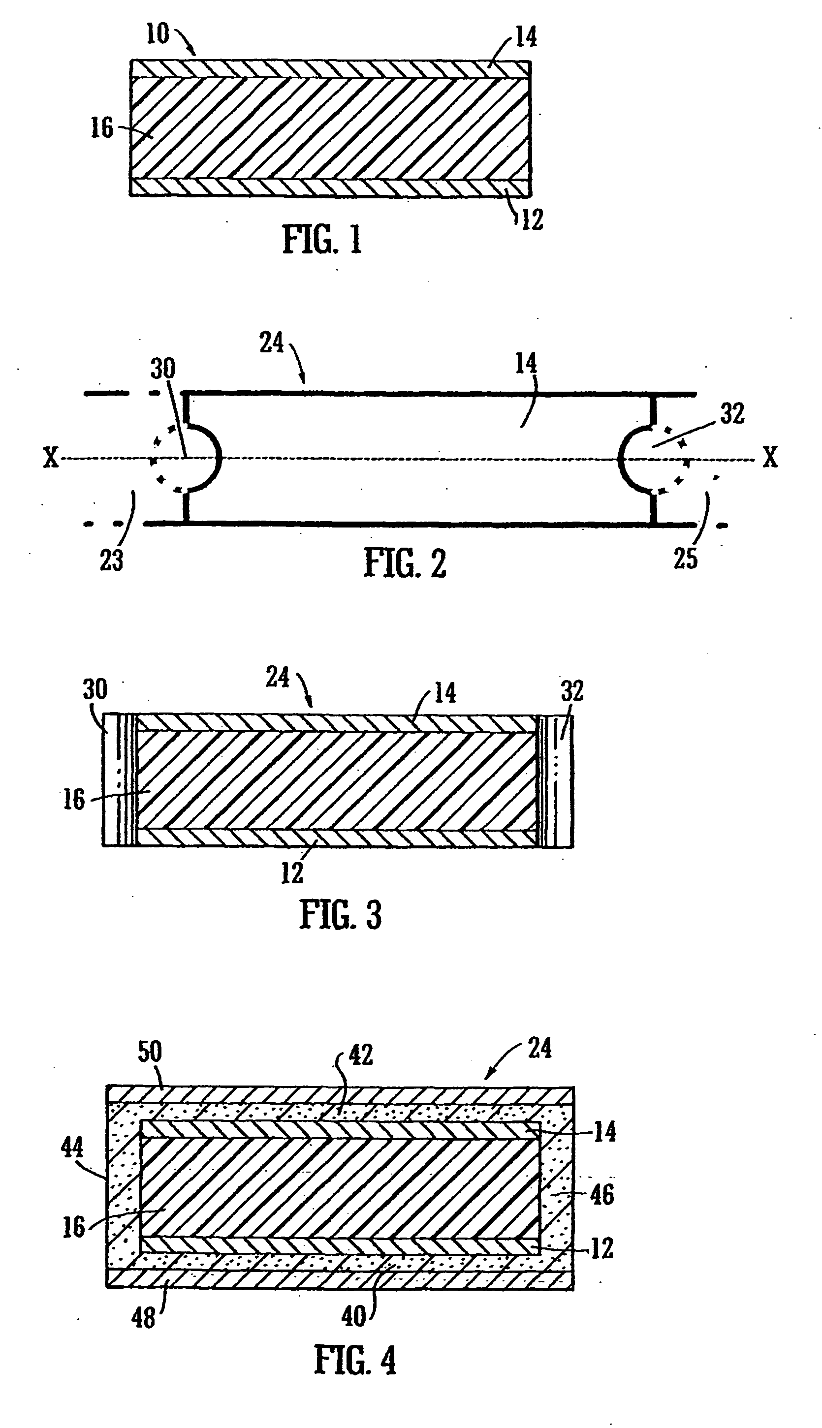
[0082] Referring now to the drawings, FIG. 1 illustrates a portion of a laminated sheet 10 that may be provided as an initial step in the process of manufacturing an electronic device in accordance with the present invention. The sheet 10 comprises two layers of metal foil 12, 14 and a region of active device material, for example conductive polymer PTC material 16. Specifically, the exemplary laminated sheet 10 shown comprises a layer of conductive polymer PTC material 16 sandwiched between a first or lower layer of metal foil 12 and a second or upper layer of metal foil 14.

[0083] The layer of conductive polymer PTC material 16 may comprise any suitable PTC material, including for example any suitable conductive polymer composition. An example of a suitable conductive polymer composition would be high density polyethylene (HDPE) into which is mixed an amount of carbon black that results in the desired electrical operating characteristics. An example of such a mixture is disclosed ...


PUM


Abstract

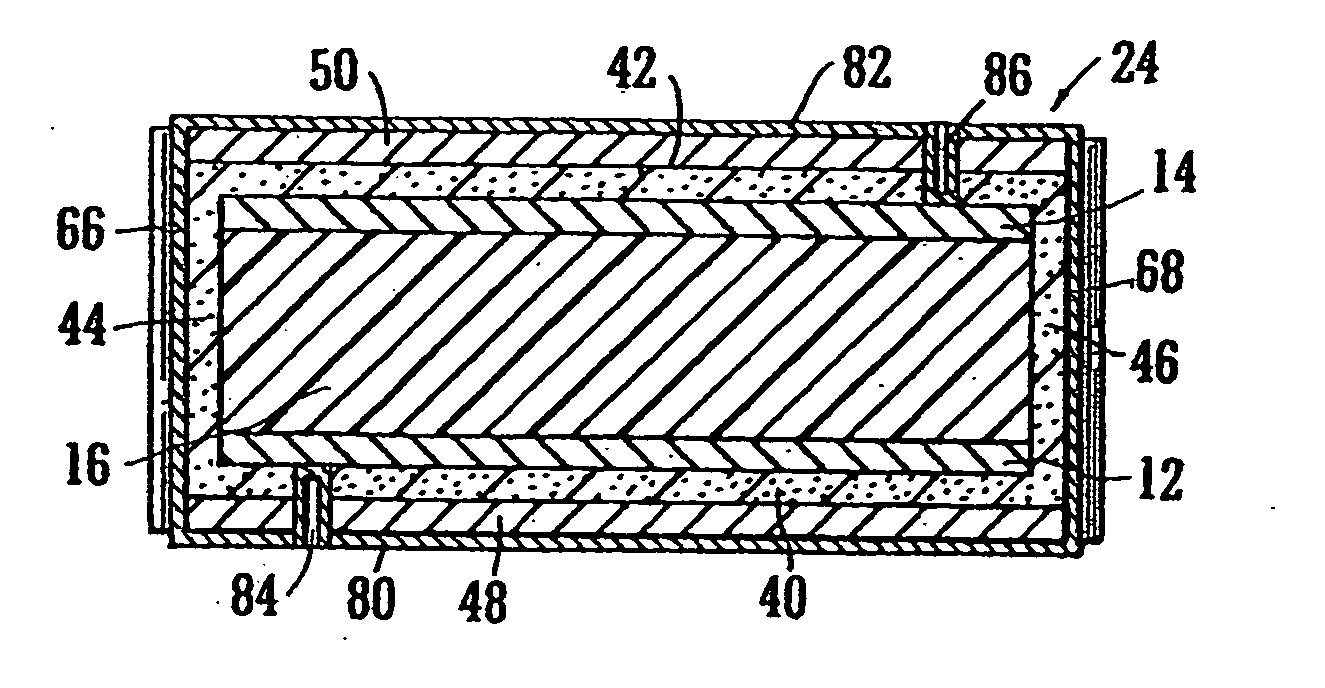
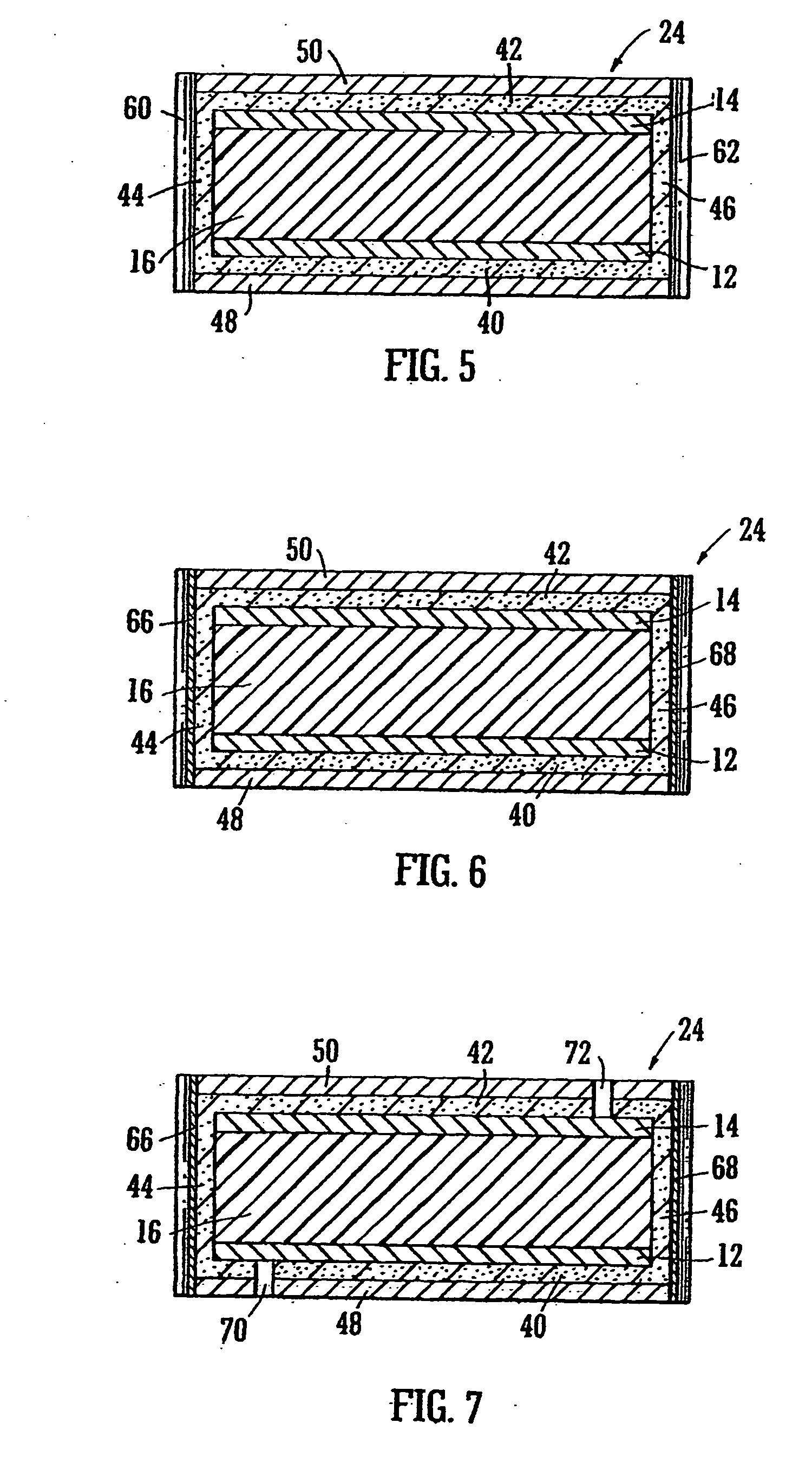
An electronic device is manufactured using printed circuit board manufacturing processes. In particular, a laminar device comprises a first metal layer (12), a second metal layer (14), at least one layer of device material sandwiched between the first and second metal layers. A first layer of insulating material (40) substantially covers the first metal layer (12). A third metal layer (48) is provided on the first layer of insulating material (40). This third metal layer (48) is divided to provide a first terminal (90) and a second terminal (92). The first terminal (90) is electrically connected to the first metal layer (12) by a conductive interconnect (84) formed through said first layer of insulating material (40), and the second terminal (92) is electrically connected to said second metal layer (14) by a conductive path (68) comprising an insulated conductive channel which passes through and is insulated from said first metal layer (12) and said at least one layer of device material (16). The use of an insulated channel provides a cost effective method of manufacture and maximizes the effective area of device material used. A PTC component is built through this method.

Description

CROSS-REFERENCES TO RELATED APPLICATIONS [0001] This application is related to PCT / US2003 / 007875 (WO2004 / 053899), which claims the benefit of U.S. Provisional Application No. 60 / 432,493, filed on Dec. 11, 2002. This application is also related to U.S. patent application Ser. No. ______ (Attorney docket no. 025959-000100US), which is being filed on the same day as the present application. All of the above applications are herein incorporated by reference in their entirety for all purposes.BACKGROUND OF THE INVENTION [0002] The present invention relates generally to the field of electronic devices. More specifically, this invention relates to positive temperature coefficient (PTC) devices that are designed for overcurrent protection and can be surface mounted in printed circuit board (PCB) applications. [0003] It is well known that the resistivity of many conductive materials changes with temperature. For example, the resistivity of a PTC material increases as the temperature of the m...

Claims


Application Information

Patent Timeline
IPC IPC(8): H01C7/13H01C1/14H01C1/148H01C7/02H01C17/28
CPCH01C1/1406H01C1/148H01C7/02H01C7/027H01C17/28H05K1/0206H05K1/056H05K3/0052H05K3/403H05K3/429H05K3/44H05K3/445H05K2201/09181H05K2201/09554H05K2201/09845
Inventor BJORSELL, STEN
Owner BJORSELL STEN
Learn More