Shadow mask deposition system for and method of forming a high resolution active matrix liquid crystal display (LCD) and pixel structures formed therewith

a liquid crystal display and shadow mask technology, applied in the field of shadow mask deposition system for high-resolution active matrix liquid crystal display (lcd) and the formation of pixel structures therewith, can solve the problems of limited resolution achievable through shadow mask deposition process, high cost and complexity, and high cos

Inactive Publication Date: 2006-07-13
ADVANTECH GLOBAL LTD
View PDF11 Cites 45 Cited by
  • Summary
  • Abstract
  • Description
  • Claims
  • Application Information

AI Technical Summary

Benefits of technology

[0022] Lastly, the invention is an LCD pixel that includes a first conductive segment connected to a first bus; a first insulator segment on the first conductive segment; a second conductive segment on the first insulator segment; a liquid crystal material on the second conductive segment; a third conductive segm

Problems solved by technology

Because of the number of steps required to form an active matrix backplane by use of the photolithography manufacturing process, foundries of adequate capacity for volume production of backplanes are very expensive.
However, the resolution achievable via the shadow mask deposition process is limited.
Because of this demand for higher resolution, active matrix backplane manufacturers have migrated away from the less costly and less complex shadow mask deposition process in favor of the photolithography process, but at

Method used


Image

  • Shadow mask deposition system for and method of forming a high resolution active matrix liquid crystal display (LCD) and pixel structures formed therewith
  • Shadow mask deposition system for and method of forming a high resolution active matrix liquid crystal display (LCD) and pixel structures formed therewith
  • Shadow mask deposition system for and method of forming a high resolution active matrix liquid crystal display (LCD) and pixel structures formed therewith

Examples


Embodiment Construction

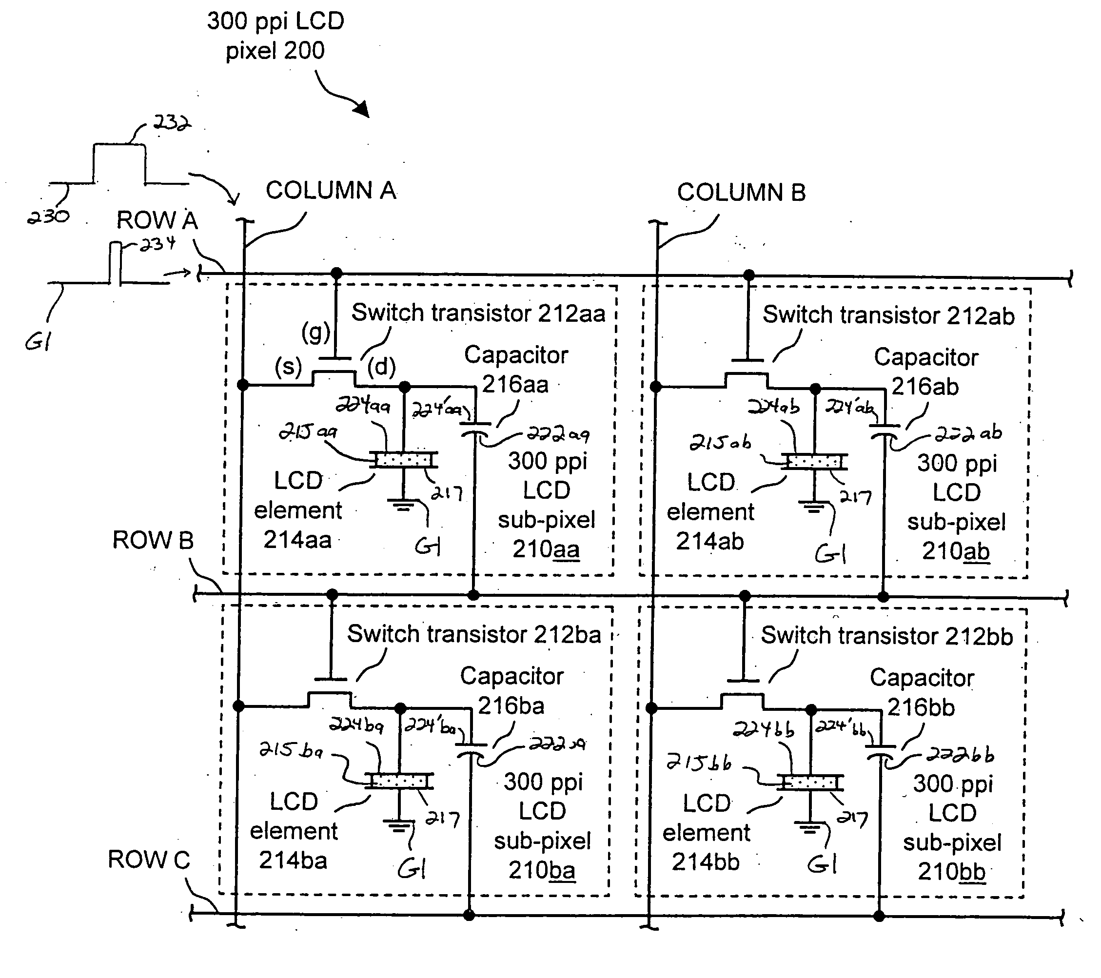
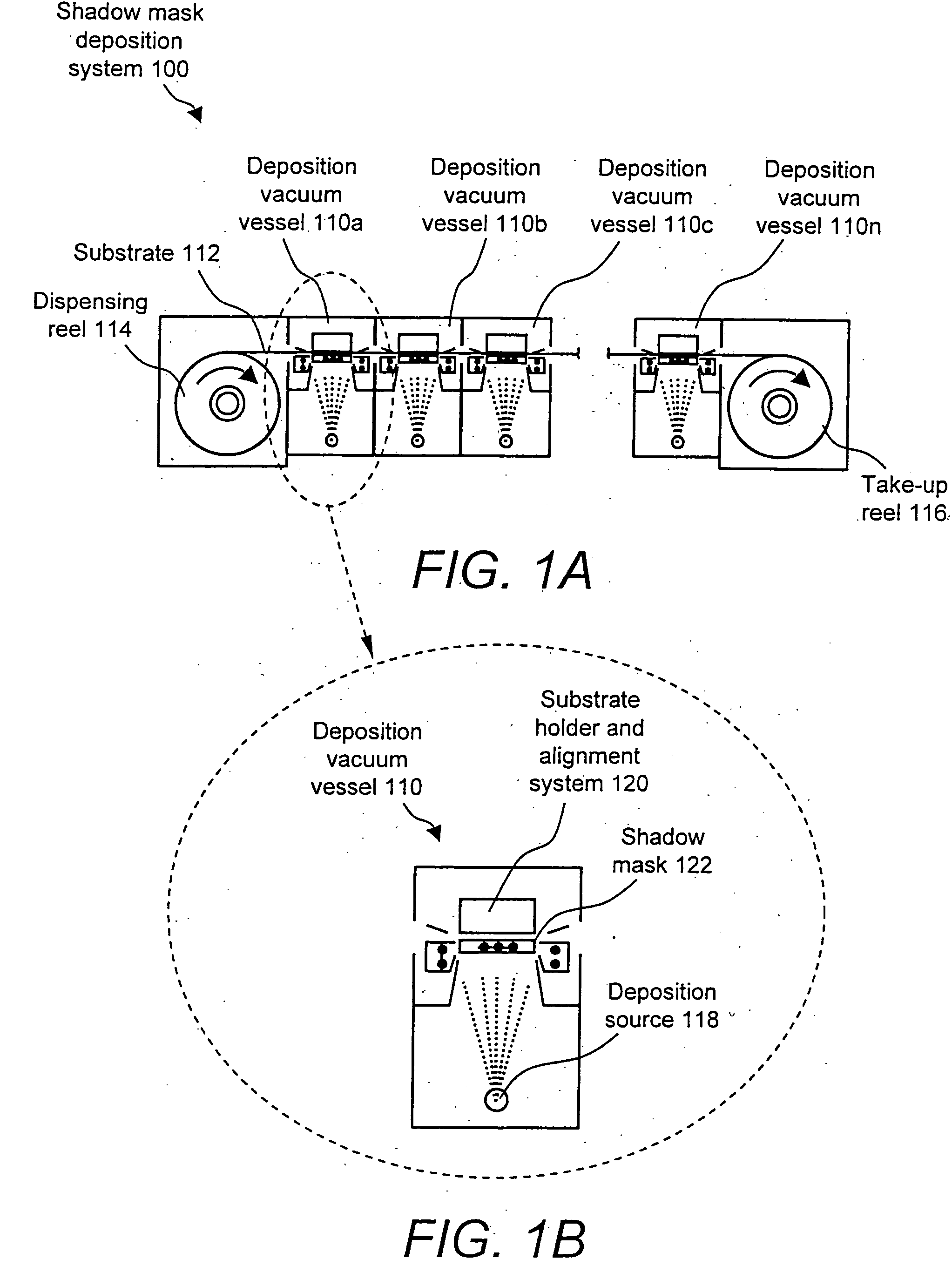
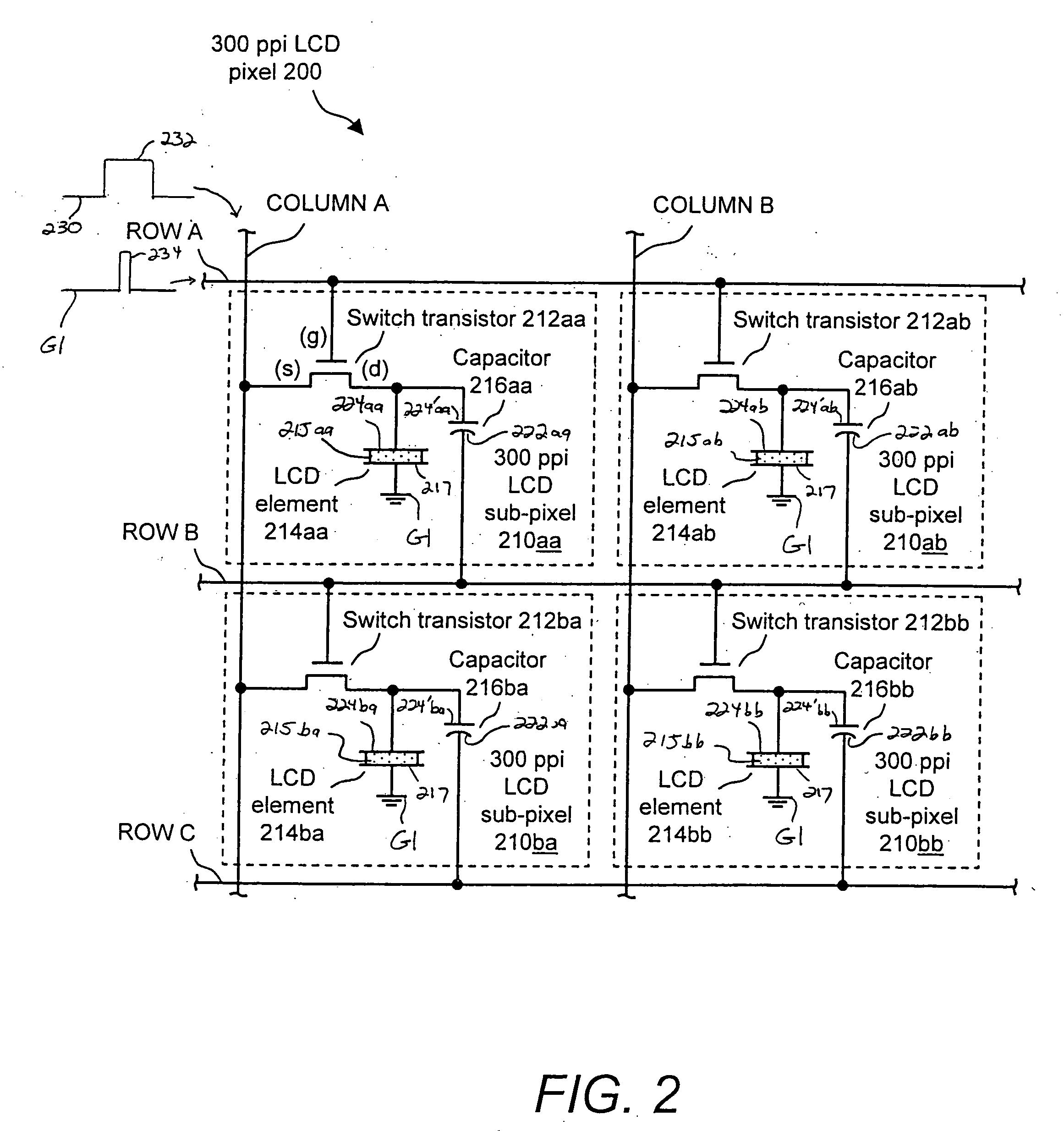
[0036] The present invention will be described with reference to the accompanying figures where like reference numbers correspond to like elements.

[0037] With reference to FIGS. 1A and 1B, a shadow mask deposition system 100 for forming LCD pixels of a high resolution active matrix LCD includes a plurality of deposition vacuum vessels 110 (e.g., deposition vacuum vessels 110a through 110n). The number and arrangement of deposition vacuum vessels 110 is dependent on the number of deposition events and etching events required for any given product formed therewith.

[0038] In use of shadow mask deposition system 100, a substrate 112 translates through the serially arranged deposition vacuum vessels 110 by use of a reel-to-reel mechanism that includes a dispensing reel 114 and a take-up reel 116.

[0039] Each deposition vacuum vessel 110 includes a deposition source 118, a substrate holder and alignment system 120 and a shadow mask 122. For example, deposition vacuum vessel 110a include...


PUM


Abstract

An LCD pixel includes a first conductive segment connected to a first bus, a first insulator segment on the first conductive segment, a second conductive segment on the first insulator segment, a liquid crystal material on the second conductive segment, a third conductive segment on the liquid crystal material, and a thin film transistor having a control terminal, a first power terminal and second power terminal connected to a second bus, a third bus and the second conductive segment, respectively. In response to application of a suitable signal on the second bus when reference voltages are present on the first bus and on the third conductive segment, and a voltage is applied to the third bus, the thin film transistor is operative for charging a capacitor formed by the first conductive segment, the first insulator segment and the second conductive segment and for activating the liquid crystal material.

Description

BACKGROUND OF THE INVENTION [0001] 1. Field Of The Invention [0002] The present invention relates to liquid crystal displays (LCDs) and, more particularly, to forming a high resolution active matrix LCD by a shadow mask deposition process. [0003] 2. Description Of Related Art [0004] Active matrix backplanes are widely used in flat panel displays, such as LCDs, for routing signals to pixels of the display in order to produce viewable pictures. Presently, such active matrix backplanes are formed by use of a photolithography manufacturing process, which has been driven in the market by the demand for higher and higher resolution displays which are not otherwise possible with other manufacturing processes. Photolithography is a pattern definition technique that uses electromagnetic radiation, such as ultraviolet (UV) radiation, to expose a layer of resist that is deposited on the surface of a substrate. Exemplary photolithography processing steps to produce an active matrix backplane in...

Claims


Application Information

Patent Timeline
IPC IPC(8): G02F1/1343
CPCG02F1/1362G02F2001/136231G02F1/136231H01L27/1288
Inventor BRODY, THOMAS PETER
Owner ADVANTECH GLOBAL LTD
Why Eureka
Try Eureka