Supercharge Your Innovation With Domain-Expert AI Agents!

Tile-based routing method of a multi-layer circuit board and related structure

a multi-layer circuit board and routing method technology, applied in cross-talk/noise/interference reduction, printed circuit aspects, instruments, etc., can solve the problems of spoiling the performance of the die, the limitations of the above-mentioned packaging method, and the limited number of such pads for a given sized di

Inactive Publication Date: 2006-07-13
SILICON INTEGRATED SYSTEMS
View PDF9 Cites 4 Cited by
  • Summary
  • Abstract
  • Description
  • Claims
  • Application Information

AI Technical Summary

Benefits of technology

This method effectively reduces capacitive interference, enhances signal quality, and allows for more aggressive signal routing density without significantly increasing die size, improving the efficiency of flip-chip packaging.

Problems solved by technology

However, the above-mentioned packaging method has its limitations.
First, because only the periphery of the die is used for external connection pads, the number of such pads for a given sized die is limited.
Second, when all the pads are provided only at the die's periphery, additional routing is required to bring the corresponding signals, particularly power and ground signals, to the interior logic of the die.
Third, in wire-bond dies, the wire connections between the die and the package pins introduce additional resistance and inductance, which sometimes may spoil the die's performance.
However, even based on the flip-chip packaging technique, a basic and inevitable principle is that the die size should be subject to the size and quantity of the spreading bumpers.
Due to that nowadays, companies developing and manufacturing electronic products are challenged by a blooming market demand for smaller, more efficient, and a higher performance product, bringing down the relative die size to meet the cost concern becomes a crucial issue.
Routing the signal traces 18 from each of these bumper pads 20 to the appropriate position on the die 10 can therefore become a complicated task.
However, the higher signal trace density and lower die size will also introduce the smaller space among all the signal traces 18, which would worsen the cross-talk effect (mostly the capacitive cross-talk) between signals and bring down the signal quality.

Method used


Image

  • Tile-based routing method of a multi-layer circuit board and related structure
  • Tile-based routing method of a multi-layer circuit board and related structure
  • Tile-based routing method of a multi-layer circuit board and related structure

Examples


Embodiment Construction

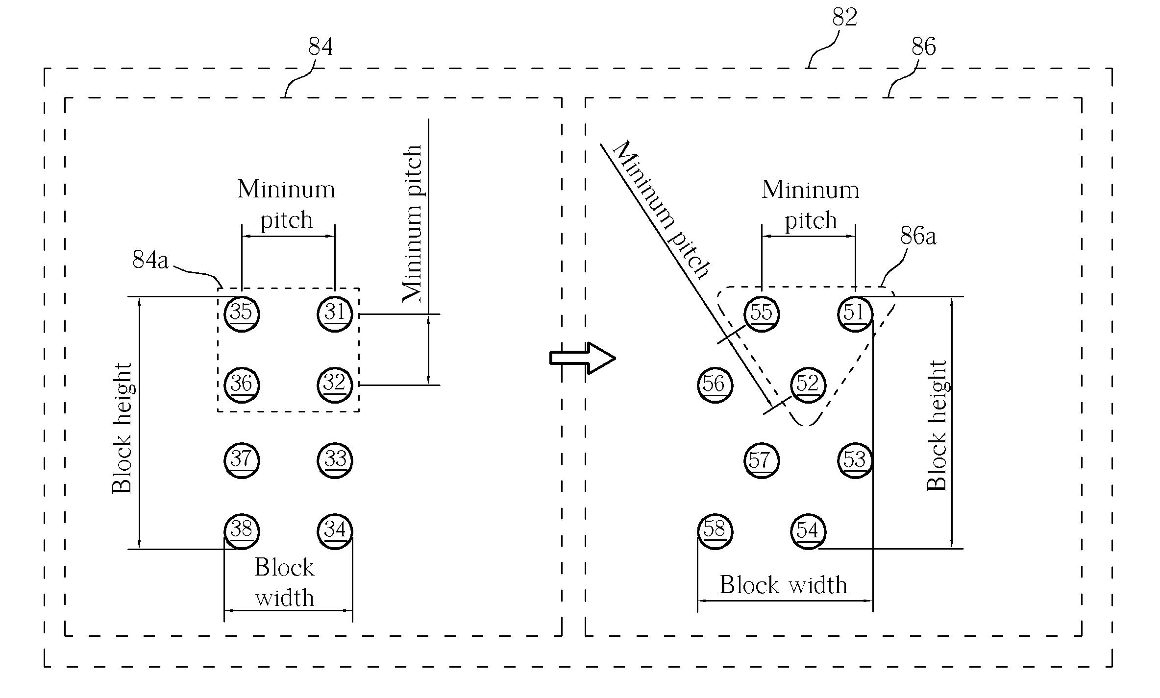
[0026] Please refer to FIG. 5, which is a schematic diagram showing a first arrangement of partial bumper pads 31-38 and a plurality of corresponding signal traces 39-46. The arrangement of the bumper pads is highly relevant to a die size of a high pin count chip. With the flip chip packaging, the die size (the embodiment of die 10 is shown in FIG. 1 and FIG. 4) is subject to 2 items, quantity of the bumper pads and a required area in which the plurality of corresponding signal traces are routed. As shown in FIG. 5, the bumper pads 31-38 are assigned on a multi-layer substrate 82. The multi-layer substrate 82 comprises at least a first layer 82A and a second layer 82B (the second layer 82B is vertically underneath the first layer 82A). The multi-layer substrate 82 can be the 6-layer build-up substrate 12 described in FIG. 2 (the first layer 82A corresponds to the build-up layer 12A, and the second layer 82B corresponds to the build-up layer 12B) or any other multi-layer circuit boar...


PUM

PropertyMeasurementUnit
widthaaaaaaaaaa
widthaaaaaaaaaa
widthaaaaaaaaaa

Abstract

A method for routing a plurality of signal traces out of a plurality of corresponding bumper pads for implementation of a die on a multi-layer circuit board includes utilizing the plurality of bumper pads positioned in a periphery area of the die; utilizing a plurality of power / ground bumper pads positioned in a center area of the die; assigning a plurality of signal traces corresponding to a plurality of bumper pads as a plurality of first-layer traces being routed in a first layer of the multi-layer circuit board; assigning a plurality of signal traces corresponding to a plurality of bumper pads as a plurality of second-layer traces being routed in a second layer of the multi-layer circuit board; routing the plurality of first-layer traces straight away from the die; and routing the plurality of second-layer traces with a turn not to be vertically underneath the first-layer traces.

Description

CROSS REFERENCE TO RELATED APPLICATIONS [0001] This application is a division of U.S. application Ser. No. 10 / 604,036 filed Jun. 23, 2003, the contents of which are herein incorporated by reference in their entirety.BACKGROUND OF THE INVENTION [0002] 1. Field of the Invention [0003] The present invention relates to a routing method for routing a plurality of signal traces out of corresponding bumper pads in a multi-layer circuit board, and more particularly, to a tile-based routing method for routing a plurality of signal traces and a plurality of shielding traces in the multi-layer circuit board. [0004] 2. Description of the Prior Art [0005] In modern society with developed computer technology, the computer system, which comprises a plurality of integrated circuits, has been utilized in a broad spectrum of fields. For example, household appliances with automatic control systems, mobile communication devices, and personal computers utilize integrated circuits to perform certain func...

Claims


Application Information

Patent Timeline
Patent Type & Authority Applications(United States)
IPC IPC(8): H01L21/50G06F17/50H01L23/498H01L23/50H01L23/552H05K1/02H05K1/11
CPCG06F17/5077Y10T29/49128H01L23/49838H01L23/50H01L23/552H01L2924/15173H05K1/0219H05K1/112H05K2201/09227H05K2201/09236H05K2201/10674H01L2924/0002H01L23/49822Y10T29/49117Y10T29/49155Y10T29/49126Y10T29/49147H01L2924/00G06F30/394
Inventor FANG, CHUNG-YICHAO, TZE-HSIANGSU, YI-SHOW
Owner SILICON INTEGRATED SYSTEMS
Features
  • R&D
  • Intellectual Property
  • Life Sciences
  • Materials
  • Tech Scout
  • Unparalleled Data Quality
  • Higher Quality Content
  • 60% Fewer Hallucinations
Learn More