Semiconductor device and manufacturing method of the same

a semiconductor device and manufacturing method technology, applied in the field of semiconductor devices, can solve the problems of reducing the cell pitch of power mos-fets and reducing their on-resistance, and achieve the effect of suppressing or preventing the operation of parasitic elements reducing the on-resistance of the semiconductor device, and reducing the resistance of the semiconductor devi

Active Publication Date: 2006-07-20
RENESAS ELECTRONICS CORP
View PDF2 Cites 90 Cited by
  • Summary
  • Abstract
  • Description
  • Claims
  • Application Information

AI Technical Summary

Benefits of technology

[0016] A semiconductor device having a field-effect transistor with a trench gate structure is so constructed that the relation expressed as b≦a holds, where a is the distance between an end of the insulating layer in the upper face of the source region and the end of the upper face of the source region farther from the gate electrode; and b is the length of the overlap between the insulating layer and the upper face of the source region. Thus, the on-resistance of the semiconductor device can be reduced.
[0017] A semiconductor device having a field-effect transistor with a trench gate structure is so constructed that the following is implemented: a cutoff trench is formed between an end of a source region on the periphery of a group of multiple cells of the field-effect transistor with a trench gate structure and an end of an insulating layer formed outside the end of the source region on the periphery of the group of the multiple cells. Thus, the operation of parasitic elements of the semiconductor device can be suppressed or prevented.

Problems solved by technology

Therefore, it is an important problem how demand for reduction in the cell pitch of power MOS-FETs and reduction in their on-resistance should be met.

Method used


Image

  • Semiconductor device and manufacturing method of the same
  • Semiconductor device and manufacturing method of the same
  • Semiconductor device and manufacturing method of the same

Examples


first embodiment

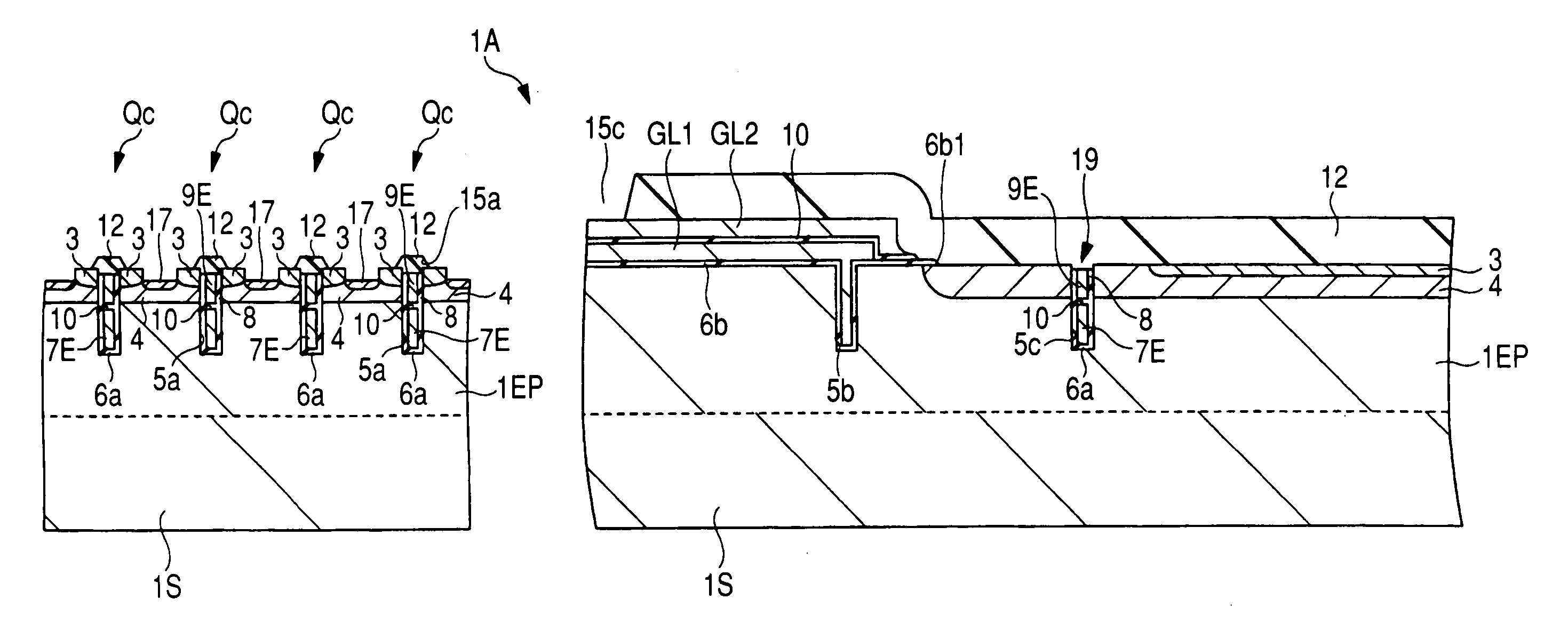
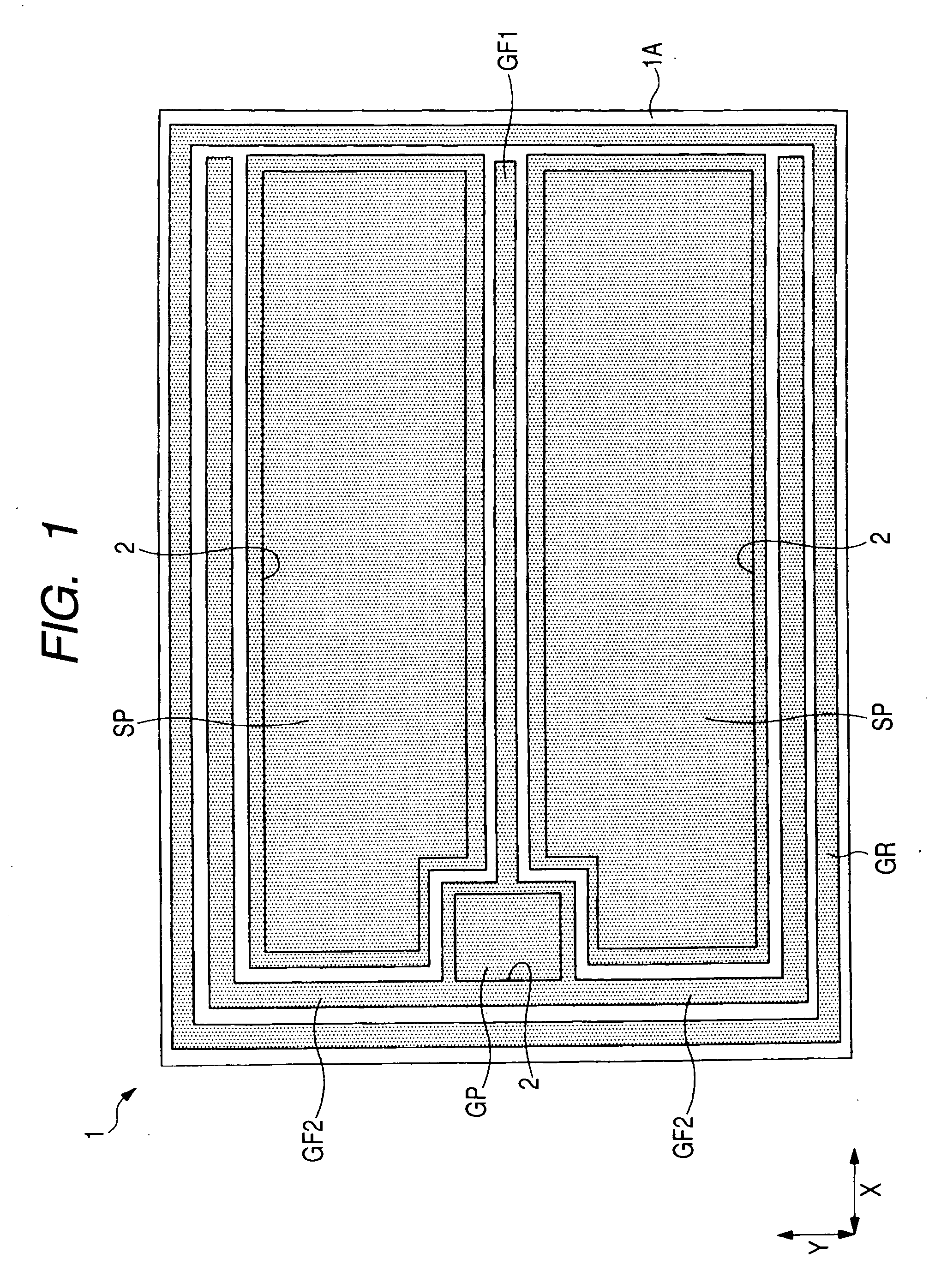
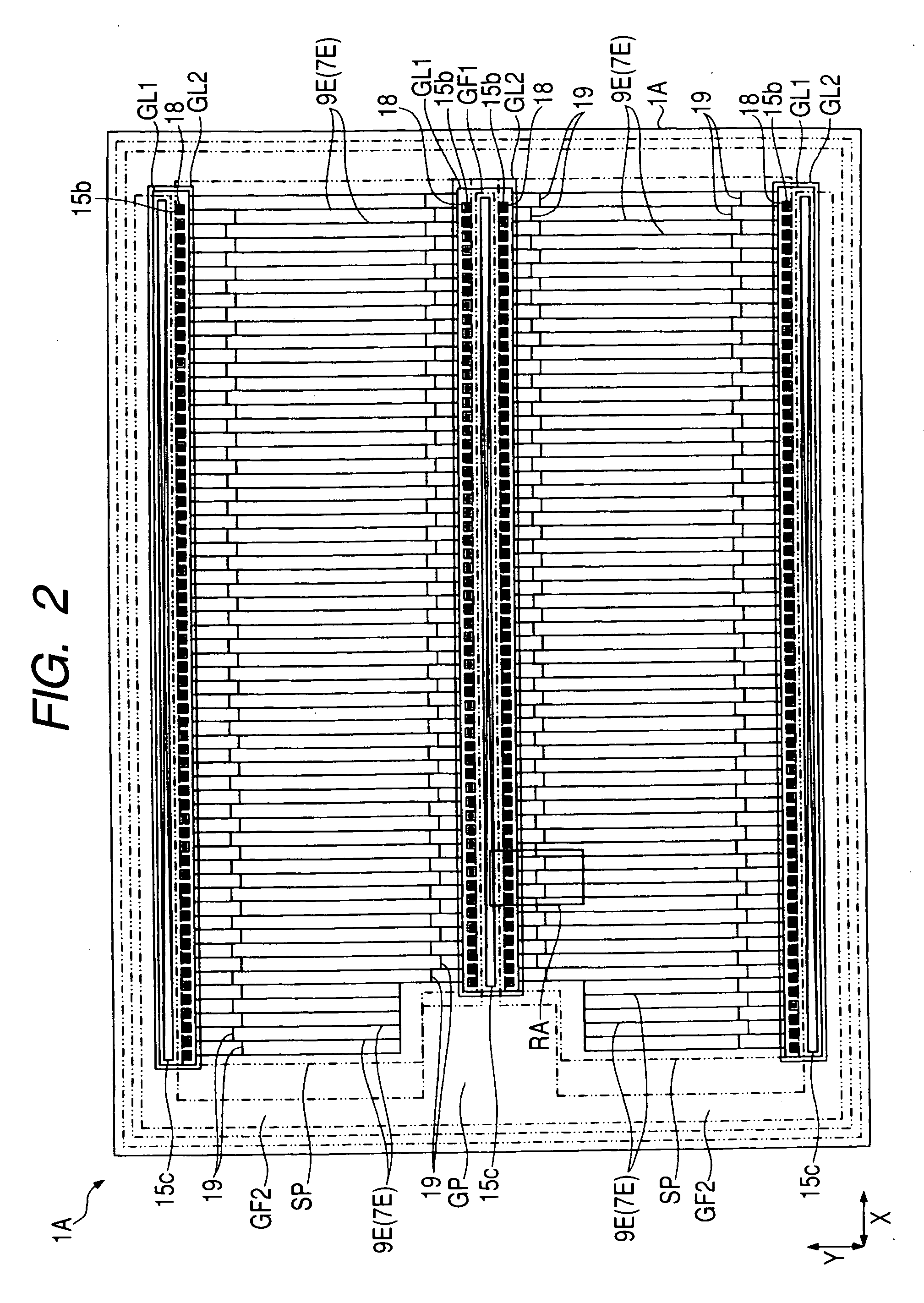
[0055]FIG. 1 and FIG. 2 are plan views of a semiconductor chip that constitutes a semiconductor device in a first embodiment; FIG. 3 is an enlarged plan view of area RA in the semiconductor chip in FIG. 2; FIG. 4 is a sectional view taken along line X1-X1 of FIG. 3; FIG. 5 is an enlarged sectional view of a substantial part of the semiconductor chip in FIG. 4; FIG. 6 is an enlarged plan view of a substantial part of the semiconductor chip in FIG. 3; and FIG. 7 is a sectional view taken along line Y1-Y1 of FIG. 3. Code Y indicates a first direction, and code X indicates a second direction orthogonal to the first direction. The first direction Y is equivalent to the direction of the short sides of the semiconductor chip. It is also equivalent to the direction of the length (extension) of the gate electrode of a power MIS-FET (Metal Insulator Semiconductor-Field Effect Transistor) The second direction X is equivalent to the direction of the length of the semiconductor chip, and is also...

second embodiment

[0093] Description will be given to the above-mentioned cutoff portion 19 in relation to a second embodiment. The configuration of the chip 1 is the same as described with respect to the first embodiment with reference to FIG. 1 to FIG. 7. In the following description of the second embodiment, the same members as described with respect to the first embodiment will be marked with the same numerals or codes.

[0094]FIG. 15 is a sectional view taken along line Y2-Y2 of FIG. 3. The second embodiment is provided with a cutoff portion 19. It is positioned between an end of a semiconductor region 3 for source on the periphery of a group of the multiple cells Qc of the power MIS-FET Q (position P4) and an end 6b1 of an insulating layer 6b for isolation provided outside of the end (position P4) of the semiconductor region 3 for source. The cutoff portions 19 are provided between adjoining gate electrodes 9E so that they are extended in the second direction X and intersect the gate electrodes ...

third embodiment

[0100] With respect to a third embodiment, description will be given to an example of the manufacturing method for the power MIS-FET Q, described in relation to the first and second embodiments, with reference to FIG. 20 to FIG. 36. In FIG. 20 to FIG. 36, the left part shows the element formation region (region where a group of the cells Qc of the power MIS-FET Q are to be formed), and the right part shows the peripheral region (regions including the isolation regions).

[0101] First, a substrate 1A (a planar and circular semiconductor wafer in this stage), illustrated in FIG. 20, is prepared. This substrate is obtained by growing the epitaxial layer 1EP, composed of a high-resistance n-type silicon (Si) single crystal, over the substrate portion 1S composed of a low-resistance n+-type silicon (Si) single crystal. Subsequently, an insulating layer 30 composed of, for example, silicon oxide is formed over the main surface of the substrate 1A (the upper face of the epitaxial layer 1EP)...


PUM


Abstract

The on-resistance of a semiconductor device having a power transistor with a trench gate structure is reduced. A power MIS-FET with a trench gate structure is so formed that the relation expressed as 0≦b≦a holds, where a is the distance between an end of an interlayer insulating layer over the upper face of a semiconductor region for source and the end (position on the periphery of a trench) of the upper face of the semiconductor region for source farther from the gate electrode; and b is the length of the overlap between the interlayer insulating layer and the upper face of the semiconductor region for source. (b is the distance between the position of the end of the interlayer insulating layer over the upper face of the semiconductor region for source and position on the periphery of a trench). As a result, the area of contact between source pads and the semiconductor regions for source is increased, and further the distance between the source pads and a channel forming region can be shortened. Therefore, the on-resistance of the power MIS-FET with a trench gate structure can be reduced.

Description

CROSS-REFERENCE TO RELATED APPLICATION [0001] The present application claims priority from Japanese patent application No. 2005-012236 filed on Jan. 20, 2005, the content of which is hereby incorporated by reference into this application. BACKGROUND OF THE INVENTION [0002] The present invention relates to a semiconductor device of a manufacturing technique of the same, and in particular to a semiconductor device having a power transistor with a trench gate structure and a manufacturing technique of the same. [0003] The power MOS-FET (Metal Oxide Semiconductor-Field Effect Transistor) with a trench gate structure is a vertical power transistor constructed as follows: a gate electrode is formed in a trench dug in the direction orthogonal to the main surface of a semiconductor substrate with a gate insulating layer in-between; a source region is formed in the surface part of the main surface of the semiconductor substrate; a drain region is formed on the under side of the semiconductor...

Claims


Application Information

Patent Timeline
Patent Type & Authority Applications(United States)
IPC IPC(8): H01L29/94
CPCH01L29/0653H01L29/407H01L29/4236H01L29/4238H01L29/456H01L29/66727H01L2924/0002H01L29/66734H01L29/7811H01L29/7813H01L2924/00
Inventor KACHI, TSUYOSHIHOSHINO, YOSHINORI
Owner RENESAS ELECTRONICS CORP
Why Eureka
Try Eureka