Insulated gate field-effect transistor and a method of manufacturing the same

a field-effect transistor and insulating gate technology, applied in the field of insulating gate field-effect transistors, can solve the problems of reducing the driving ability of the mis transistor, the application of the ion implantation technique and the activation anneal technique for forming a very shallow junction, and the not yet established ion implantation technique, so as to achieve the effect of precise junction depth

Active Publication Date: 2006-07-20
SONY CORP
View PDF7 Cites 126 Cited by
  • Summary
  • Abstract
  • Description
  • Claims
  • Application Information

AI Technical Summary

Benefits of technology

[0020] According to the present invention, the advantages are provided in which a steep PN junction having a stable configuration is formed below the source/drain region having the extens...

Problems solved by technology

However, the ion implantation technique and activation anneal technique for forming a very shallow junction which is applicable to the above-mentioned fine MIS transistor are not yet established.
In addition, even if the very shallow junction can be formed by utilizing the ion implantation method, owing to its thinness, its resistance value becomes large and a series resistance value of the source and the drain increases to reduce the driving ability of the MIS transistor.
However, this is inconsistent with the suppression of the short channel effect.
Hence, there is encountered a problem that a space is defined between the extension portion (the first source/drain region) and the channel layer and thus this space portion has a large resistance value in some...

Method used


Image

  • Insulated gate field-effect transistor and a method of manufacturing the same
  • Insulated gate field-effect transistor and a method of manufacturing the same
  • Insulated gate field-effect transistor and a method of manufacturing the same

Examples


Embodiment Construction

[0041] Preferred embodiments of the present invention will hereinafter be described by giving a CMOS device in which an NMOS transistor and a PMOS transistor are formed on the same substrate as an example with reference to the accompanying drawings.

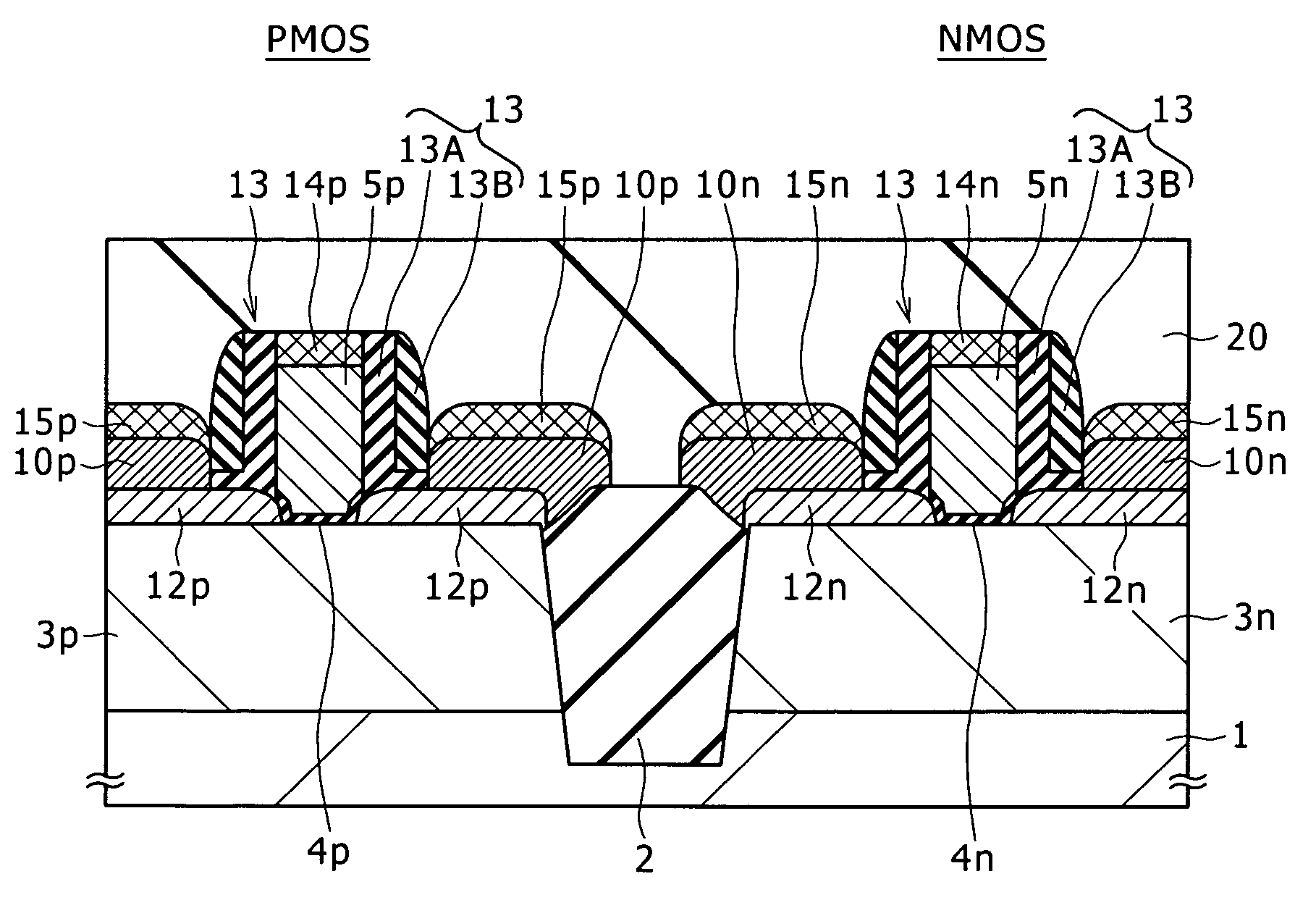
[0042]FIG. 1 is a cross sectional view of a CMOS device in a channel direction.

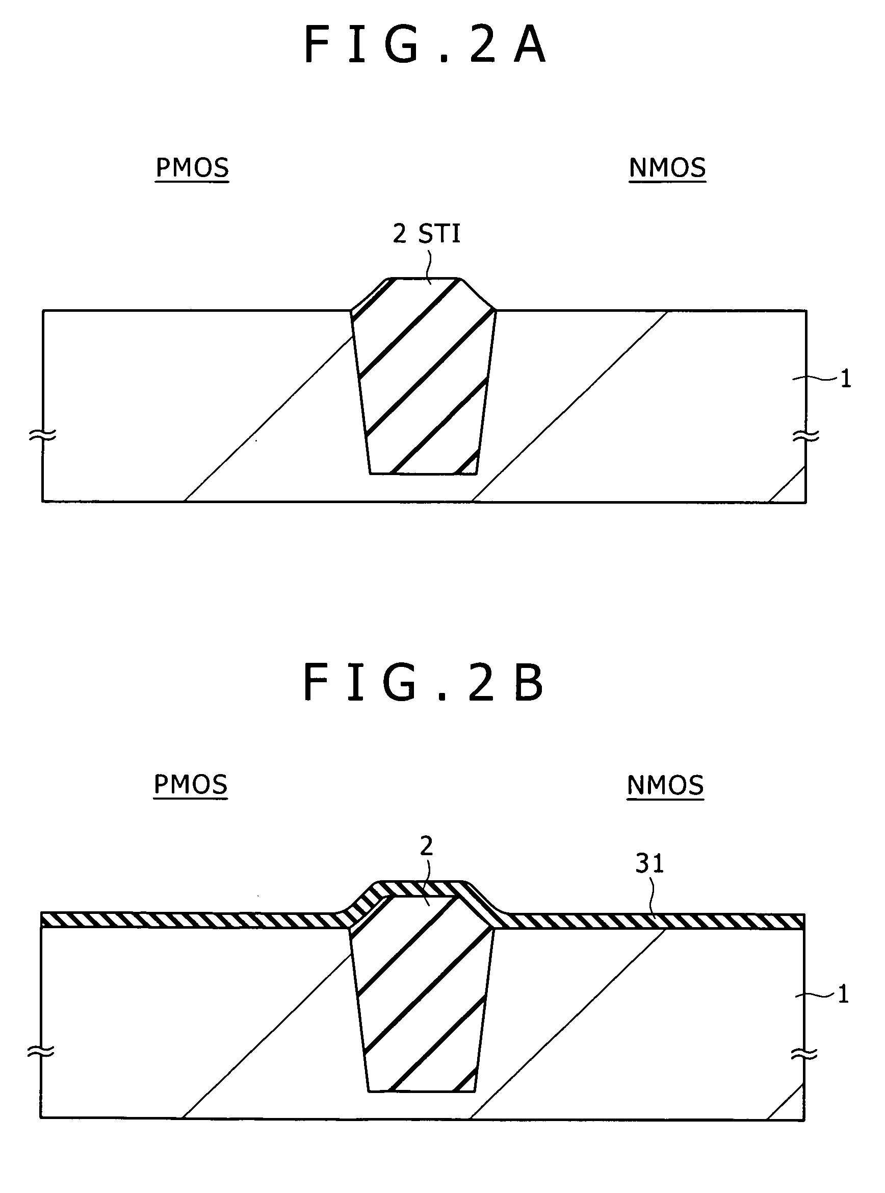
[0043] In the CMOS device shown in the figure, an isolation insulating layer, e.g., a Shallow Trench Isolation (STI) 2 is formed in a surface portion of a substrate 1 formed from a silicon wafer for example. Germanium (Ge), a compound of Ge and silicon (Si), or strain silicon may also be used as a material of the substrate 1 in addition to Si.

[0044] A P-type region (e.g., a P-type well 3n) and an N-type region (e.g., an N-type well 3p) in which inversion layers of channels are formed, respectively, are formed in a region (active region) in which no STI 2 is formed. The P-type well 3n is a substrate region in which the NMOS transistor is formed, and the N-typ...


PUM


Abstract

The invention aims at precisely making an effective junction depth sufficiently small with respect to a substrate surface having a steep PN junction stable in its configuration and having a channel formed therein in relation to an extension portion. Gate electrodes are formed on a P-type well and an N-type well through respective gate insulating films. Two extension portions are formed from two first epitaxial growth layers which contact regions, of the P-type well and the N-type well, where channels are to be formed, respectively, and which are at a distance from each other. Two second epitaxial growth layers are formed on the first epitaxial growth layers in positions which are further at a distance from facing ends of the two extension portions in a direction of being separate from each other. Thus, two source/drain regions are formed on a PMOS side and on an NMOS side each. In the case of this structure, there is adopted no ion implantation for introducing impurities into a deep portion. Hence, the impurities in the extension portions do not thermally diffuse into the substrate side through the activation anneal.

Description

CROSS REFERENCES TO RELATED APPLICATIONS [0001] The present invention contains subject matter related to Japanese Patent Application P2005-001608 filed in the Japanese Patent Office on Jan. 6, 2005, the entire contents of which being incorporated herein by reference. BACKGROUND OF THE INVENTION [0002] The present invention relates to an insulated gate field-effect transistor having an extension portion in each of two source / drain regions through which a current is supplied to a region of a semiconductor substrate which faces a gate electrode through a gate insulating film and which has a channel formed therein, and a method of manufacturing the same. [0003] With respect to the scaling of an insulated gate field-effect transistor (hereinafter referred to as “a MIS transistor”), in the International Technology Roadmap for Semiconductors (ITRS), a transistor gate length Lg of a technology node hp32 is expected to become equal to or shorter than 20 nm. [0004] In order to realize such a ...

Claims


Application Information

Patent Timeline
IPC IPC(8): H01L29/94
CPCH01L21/28114H01L21/823814H01L21/823878H01L29/165H01L29/42376H01L29/66507H01L29/66545H01L29/6656H01L29/66628H01L29/66636B65F1/16B65F2001/1653
Inventor TATESHITA, YASUSHI
Owner SONY CORP
Why Eureka
Try Eureka