Electronic circuit including at least one first and one second differential pair with the transistors sharing one and the same well

a technology of differential pair and transistor, applied in the direction of pulse generator, electric pulse generator circuit, pulse technique, etc., can solve the problems of limiting the performance of differential vco, well interfering with the operation of an amplifying stage that includes the pair, and lack of uniformity, so as to reduce parasitic capacitance and the occupied semiconductor surface in the circuit.

Active Publication Date: 2006-07-20
ATMEL CORP
View PDF7 Cites 169 Cited by
  • Summary
  • Abstract
  • Description
  • Claims
  • Application Information

AI Technical Summary

Benefits of technology

[0033] In this way, combining the transistors of the differential pairs in a single well makes it possible to obtain circuits based on differential pairs that have parasitic capacitances, particularly bottom and sidewall capacitances, and an occupied semiconductor surface that are clearly smaller compared with conventional circuits.
[0039] Implementing a double transistor of this kind can make it possible to further reduce the parasitic capacitances and the occupied semiconductor surface in the circuit.

Problems solved by technology

In fact, a lack of uniformity in respect of the dimensions of the transistors of a differential pair (for example the pair 314 in FIG. 3) generates an offset voltage between the two inputs of the pair (311 and 312) that may well interfere with the operation of an amplifying stage that includes the pair.
Unfortunately, a first drawback of this conventional arrangement is that it generates parasitic capacitances (capacitances due to the metal strips connecting the transistors, diffusion capacitance of the transistors, bottom or sidewall capacitance between the wells of the transistors and the substrate, etc) that restrict the performance of the differential VCO, in particular by reducing its oscillation frequency.
One drawback of differential VCOs is, according to the man skilled in the art, that they are unable to operate at significant frequencies (above 300 MHz, in very small-scale technologies, in other words below 0.5 μm).
Indeed, the person skilled in the art considers that, should it be required to make a differential VCO operating at these frequencies from a technology below 0.5 μm, the transistors of the differential pairs of this differential VCO would be too small to ensure good uniformity in the dimensions of the transistors of the VCO despite the use of the “crossed pairs” arrangement.

Method used


Image

  • Electronic circuit including at least one first and one second differential pair with the transistors sharing one and the same well
  • Electronic circuit including at least one first and one second differential pair with the transistors sharing one and the same well
  • Electronic circuit including at least one first and one second differential pair with the transistors sharing one and the same well

Examples


first embodiment

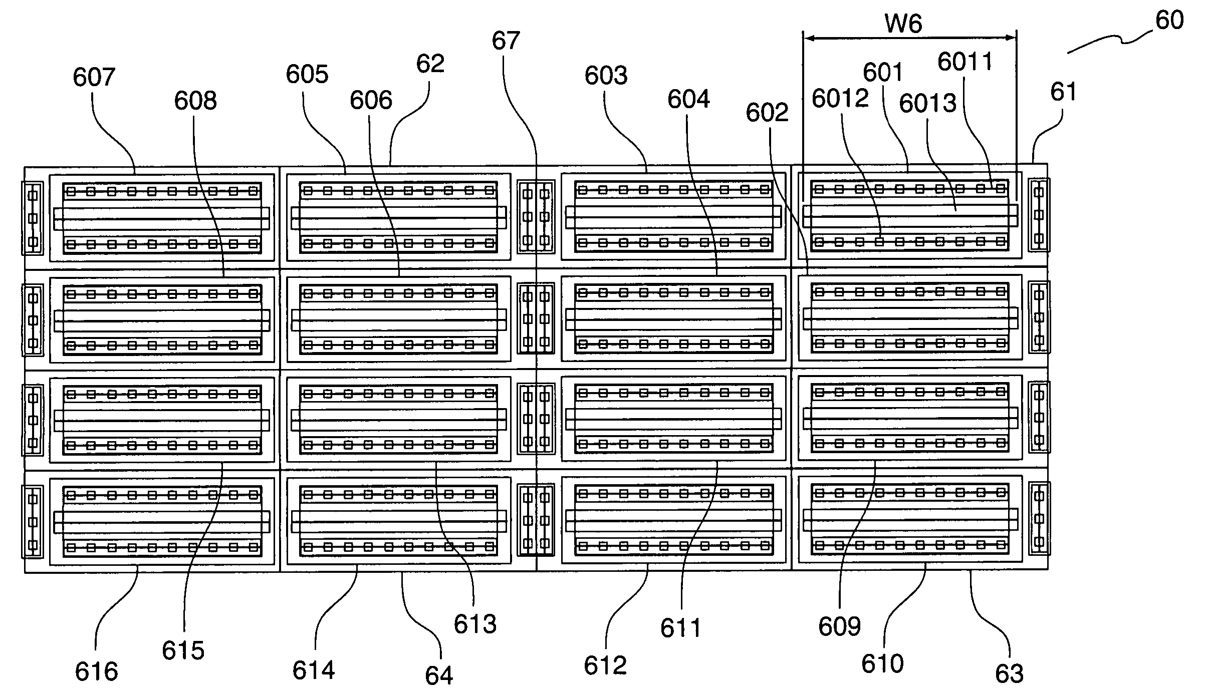
[0060] A diagram is shown in relation to FIG. 6 of the topology of the transistors of a differential VCO 60 according to the invention in which the transistors are arranged as “crossed pairs”.

[0061] The VCO 60 also includes sixteen P-type MOS transistors 601 to 616, forming first 601, 605, 609, 613, second 602, 606, 610, 614, third 603, 607, 611, 615 and fourth 604, 608, 612, 616 transistors of four differential pairs 61 to 64 (the other components of the VCO 60 are not shown in this FIG. 6).

[0062] For example, the first transistor 601 of the differential pair 61 of the VCO 60 has a source 6011, a drain 6012, and a gate 6013.

[0063] Unlike the topology of the conventional differential VCO 50 (FIG. 5), in the topology according to this first embodiment of the invention, the four differential pairs 61 to 64 are manufactured in one and the same and single well 67.

[0064] In this way, this topology according to the first embodiment of the invention makes it possible to substantially re...

second embodiment

[0076] A diagram is presented in relation to FIG. 7 of the topology of the transistors of a differential VCO 70 according to the invention, in which the transistors are not arranged as “crossed pairs”.

[0077] This VCO 70 includes eight P-type MOS transistors 711, 721, 731, 741, 712, 722, 732, 742, forming first 711, 721, 731, 741 and second 712, 722, 732, 742 transistors of four differential pairs 71 to 74 (the other components of the VCO 70 are not shown in this FIG. 7).

[0078] The first 711 and second 712 transistors of the differential pair 71 of the VCO 70 each have a source 715, 716 respectively and a gate 717, 718 respectively.

[0079] In the same way as in the topology of the differential VCO 60 according to the first embodiment of the invention (FIG. 6), in the topology according to the second embodiment of the invention, the four differential pairs 71 to 74 are manufactured in one and the same and single well 76.

[0080] However, unlike the differential VCO 60 in FIG. 6, in wh...


PUM


Abstract

The disclosure relates to an electronic circuit including at least one first and one second differential pair each including a plurality of transistors. All the transistors of said first and second differential pair are included in a single well.

Description

FIELD OF THE DISCLOSURE [0001] The field of the disclosure is that of electronic integrated circuits and more particularly that of integrated circuit design. [0002] To be more precise, the disclosure relates to the optimisation of the topology of integrated circuits, and particularly the optimisation of the topology of voltage-controlled oscillators (VCO). BACKGROUND OF THE DISCLOSURE [0003] The function of a voltage-controlled oscillator is to generate a periodic output signal, the frequency of which is a function of a continuous voltage applied to an input. It thus allows periodic signals to be generated, the frequency of which is open to selection. [0004] There are several types of voltage-controlled oscillator. A first example of a VCO is the VCO of the RC type, which is based on loading and unloading a capacitance through a capacitor. [0005] A second example of a VCO is the voltage-controlled differential oscillator, designated hereinafter as a differential VCO. The differentia...

Claims


Application Information

Patent Timeline
Patent Type & Authority Applications(United States)
IPC IPC(8): H03K3/03
CPCH01L27/0207H03F3/45179H03F3/45475
Inventor GIBET, STANISLASBENDRAOUI, ABDELLATIFMERCIER, GILLES
Owner ATMEL CORP
Why Eureka
Try Eureka