SOI wafer with cooling channels and a method of manufacture thereof

Active Publication Date: 2006-07-20
TEXAS INSTR INC
View PDF18 Cites 17 Cited by
  • Summary
  • Abstract
  • Description
  • Claims
  • Application Information

AI Technical Summary

Benefits of technology

[0008] According to one aspect of the present invention, a method of forming an SOI wafer having cooling channels formed therein is disclosed. The method comprises forming one or more cooling channels in a top surface of a first wafer, and forming a dielectric layer that will serve as the insulating layer on a top surface of a second wafer. The second wafer is treated to generate a structural weakness therein at a predetermined depth below the dielectric layer, and the top surfaces of the first and second wafers are then bonded together such that the cooling channels face the dielectric layer. A portion of the second wafer is then removed from the bonded wafer combination at a location generally corresponding to the structural weakness location. The remaining structure corresponds to a semiconductor layer (second wafer) overlying an insulating layer (second wafer) that in turn overlies a bulk semiconductor substrate (first wafer) having cooling channels therein. The cooling channels are proximate to the insulating layer, and operable to facilitate an efficient removal of heat from a device built thereon.
[0009] According to another aspect of the present invention, one or more cooling channels are formed on a top surface of the first wafer. In one example, such cooling channels are formed using a patterned etch mask overlying the first wafer such as an exposed and developed photoresist or other type mask. Using the patterned mask, an etch of the first wafer is performed, wherein one or more channels are formed in the top surface of the first wafer. Alternatively, the channels are formed via an electron beam, or an exaggerated scratching of the first wafer surface, thereby generating channels therein. The channels may then be employed to facilitate an efficient removal of heat from a completed device, wherein a cooling fluid may pass therethrough to carry away such heat.
[0013] According to yet another aspect of the present invention, a surface treatment is performed on the portion of the second wafer remaining bonded to the first wafer. In one example, the surface treatment comprises a planarization thereof, for example, by polishing to remove the surface roughness associated with the delamination. Alternatively, the exposed second wafer surface is oxidized to form a sacrificial oxide thereon, and the sacrificial oxide is then removed, thereby removing any damage associated with the delamination. Alternatively, or in addition, the second wafer surface may be exposed to a reducing ambient, wherein damage associated with the surface is repaired.
[0014] The resultant structure provides a silicon layer overlying a buried oxide, which in turn overlies a bulk silicon substrate that has cooling channels formed therein that effectively operate to channel heat away from devices formed thereon.

Problems solved by technology

These chips often become hot during operation due to heat dissipation, especially in the case of high-density logic and microprocessor chips.
One problem with the existing cooling techniques, however, is that the heat generated from any individual device or group of devices typically must travel from the device junctions through the bulk silicon to the backside of the chip where the heat sink operates to conduct the heat away therefrom.
For SOI, added to this problem is the fact that SOI devices are generally designed to run faster and can therefore generate more heat than devices on conventional bulk substrate material.

Method used


Image

  • SOI wafer with cooling channels and a method of manufacture thereof
  • SOI wafer with cooling channels and a method of manufacture thereof
  • SOI wafer with cooling channels and a method of manufacture thereof

Examples


Embodiment Construction

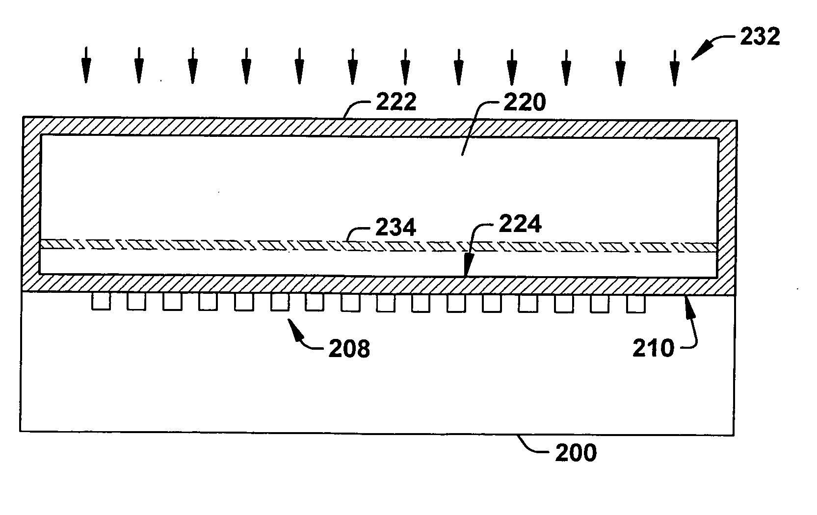
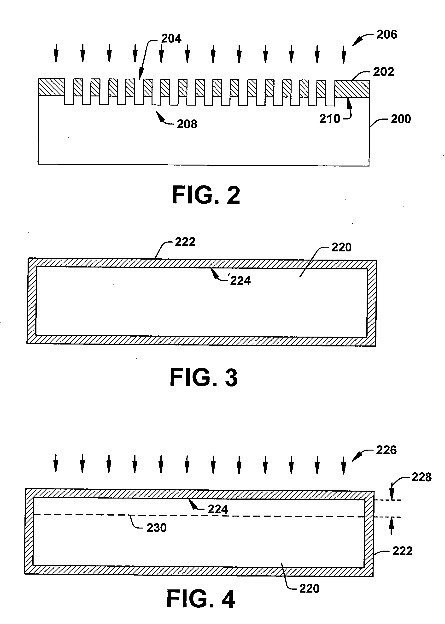
[0024] One or more implementations of the present invention will now be described with reference to the attached drawings, wherein like reference numerals are used to refer to like elements throughout. The invention relates to a method of forming an SOI wafer having cooling channels formed therein. The cooling channels facilitate an efficient removal of heat from devices formed on the wafer.

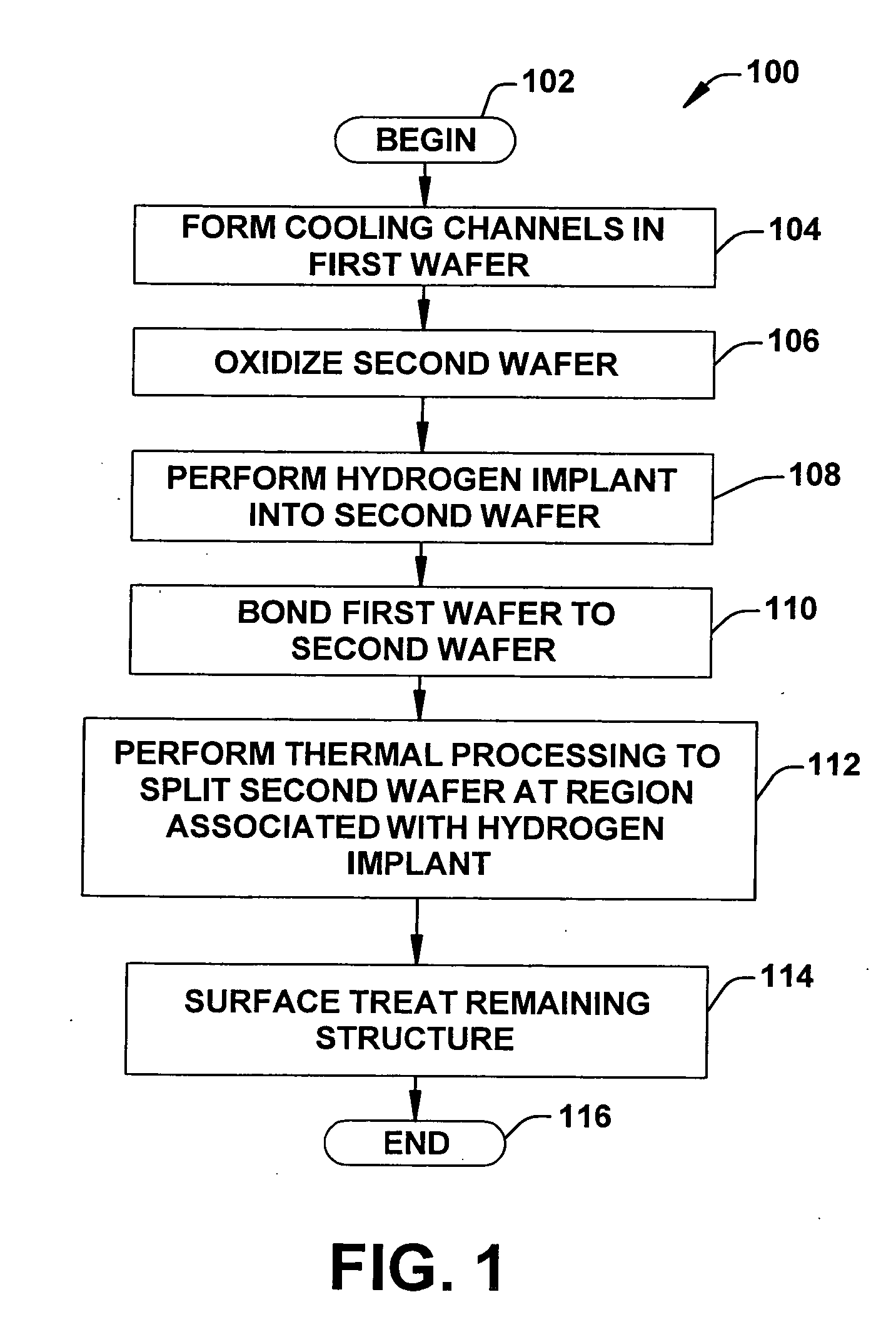
[0025] Turning now to FIG. 1, a method of forming an SOI wafer having cooling channels is illustrated and designated at reference numeral 100. Although the method 100 is illustrated and described below as a series of acts or events, it will be appreciated that the present invention is not limited by the illustrated ordering of such acts or events. For example, some acts may occur in different orders and / or concurrently with other acts or events apart from those illustrated and / or described herein, in accordance with the invention. In addition, not all illustrated steps may be required to impleme...


PUM


Abstract

A method (100) of forming a silicon-on-insulator (SOI) wafer includes forming one or more channels in a top surface of a first wafer (104), and forming an insulator layer on a second wafer (106). The second wafer is treated (108) to generate a structural weakness therein, and the first and second wafers together (110) are then bonded together so that the channels face the insulator layer. A portion of the second wafer is then removed (112) from the bonded first and second wafers at a location corresponding to the structure weakness.

Description

FIELD OF INVENTION [0001] The present invention relates generally to semiconductor device starting material, and more particularly relates to a method of making an SOI wafer with cooling channels therein. BACKGROUND OF THE INVENTION [0002] Since the development of integrated circuit technology, semiconductor chips have been fabricated primarily on a mono-crystalline silicon wafer with active devices such as transistors and diodes fabricated near the top surface of the wafer. These chips often become hot during operation due to heat dissipation, especially in the case of high-density logic and microprocessor chips. Traditionally, one method for cooling the integrated circuit chips has been the attachment of external heat sinks to the backside of the chip, or to the module into which the chip is packaged. This technology is often referred to as bulk silicon technology. [0003] A more recent technology called silicon-on-insulator, or SOI, utilizes a layer of mono-crystalline silicon sta...

Claims


Application Information

Patent Timeline
IPC IPC(8): H01L21/30H01L21/46
CPCH01L21/76254
Inventor BARNA, GABRIEL G.
Owner TEXAS INSTR INC
Why Eureka
Try Eureka