Treatment of a removed layer of silicon-germanium

a technology of silicongermanium and removal layer, which is applied in the direction of basic electric elements, electrical apparatus, semiconductor devices, etc., can solve the problems of at least partial unbonding or disbonding of the bonding interface, long post-detachment finishing step (as well as the whole removal procedure), and high cos

Inactive Publication Date: 2006-07-20
S O I TEC SILICON ON INSULATOR THECHNOLOGIES
View PDF31 Cites 22 Cited by
  • Summary
  • Abstract
  • Description
  • Claims
  • Application Information

AI Technical Summary

Benefits of technology

[0016] To achieve these benefits, the invention relates to a method for forming a semiconductor structure, which comprises providing a donor wafer that includes a first layer of Si1-xGex and a second layer of Si1-yGey located on the first layer, with x and y respectively, being in the range of 0 to 1, and x being different than y; implanting atomic species into the donor wafer to form a zone of weakness in the first layer; bonding the donor wafer to a receiver wafer; detaching the second layer and a portion of the first layer from the donor wafer by supplying energy to bonded wafers sufficient to cause cleavage at the zone of weakness to form an intermediate structure thereof; conducting a rapid thermal anneal (“RTA”) of the intermediate structure at a temperature of about 1000° C. or more for a period of time not exceeding 5 minutes; and removing any remaining portions of the first layer of the intermediate structure to provide a semiconductor structure comprising the second layer on the receiving wafer. Preferably, the remaining portions of the first layer are removed from the intermediate structure by selective etching.

Problems solved by technology

The successive actions of polishing and chemical etching, however, render the post-detachment finishing step (as well as the whole of the removal procedure) long, complex, and expensive.
Furthermore, chemical etching can in some cases result in problems with at least partial unbonding or disbonding of the bonding interface.
Thus as regards the quality of the final product, the results obtained are less than satisfactory.
That solution is not satisfactory since by substantially increasing the duration of the procedure, it still does not completely solve the problem of delamination at the edges or sides of the resulting structure.
To this end, a post-detachment stabilizing heat treatment carried out at about 1000° C. or more for several hours could be envisaged, but that solution, which is well known when producing a SOI (silicon on insulator) structure, is not suitable when transferring heterogeneous layers of Si1-xGex and Si1-yGey.
In fact, such a heat treatment causes germanium to diffuse from the layer having the highest Ge content towards the layer having the lowest Ge content, thus tending to homogenize the Ge content over the two layers so that the physical and electrical properties of those two layers can no longer be differentiated.
If the two layers become essentially identical, then subsequent etching can no longer be selective and it is not possible to remove only the first layer without removing part of the second layer.
), and low temperature reinforcement can thus only be partially effective.
Thus, the delamination problem persists even with such reinforcement.

Method used


Image

  • Treatment of a removed layer of silicon-germanium
  • Treatment of a removed layer of silicon-germanium
  • Treatment of a removed layer of silicon-germanium

Examples


Embodiment Construction

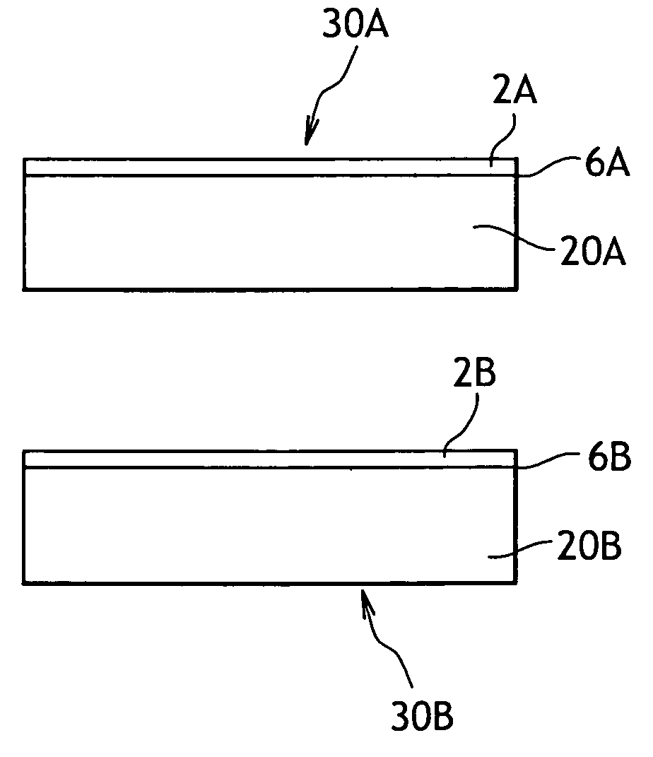
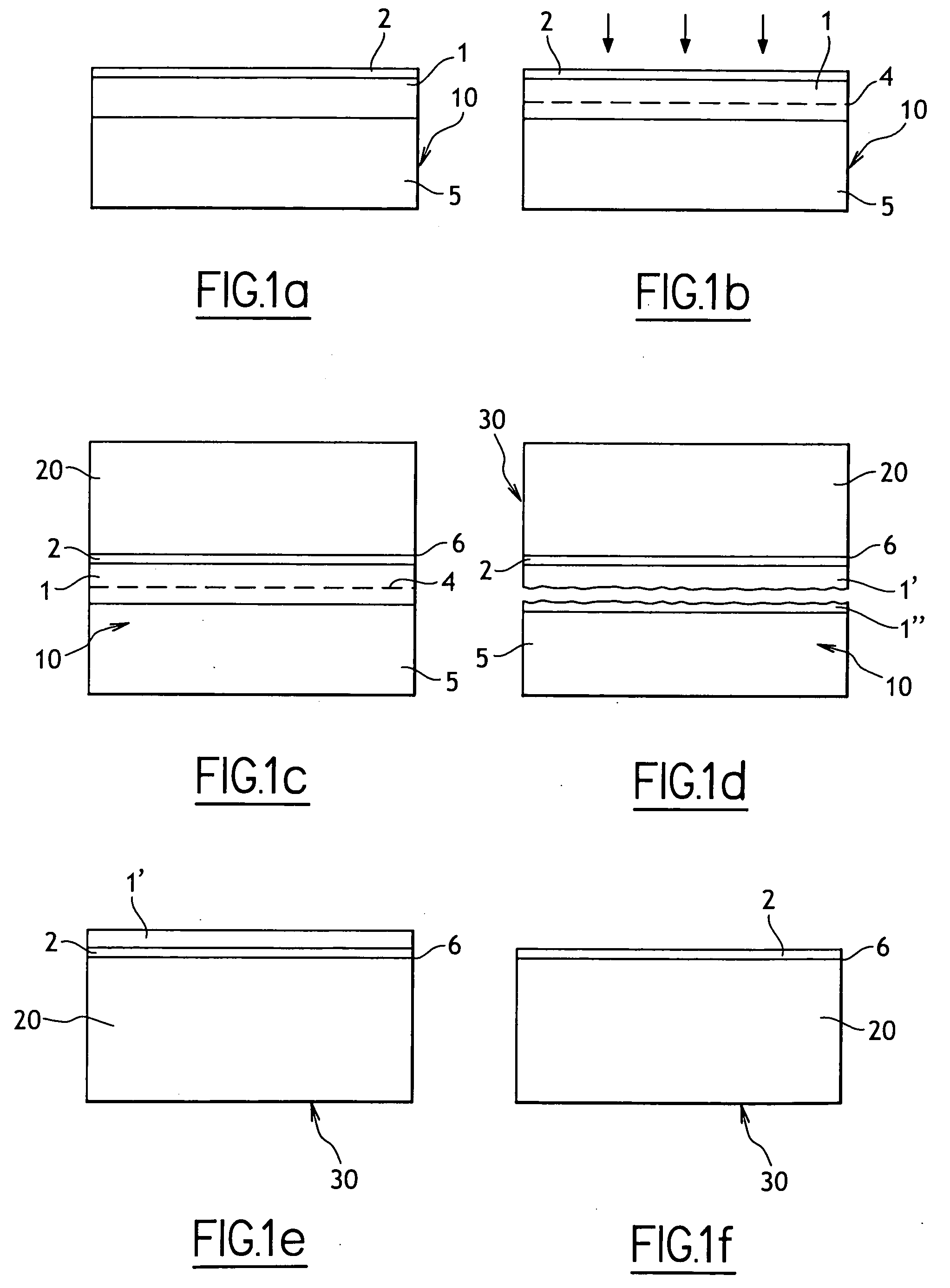
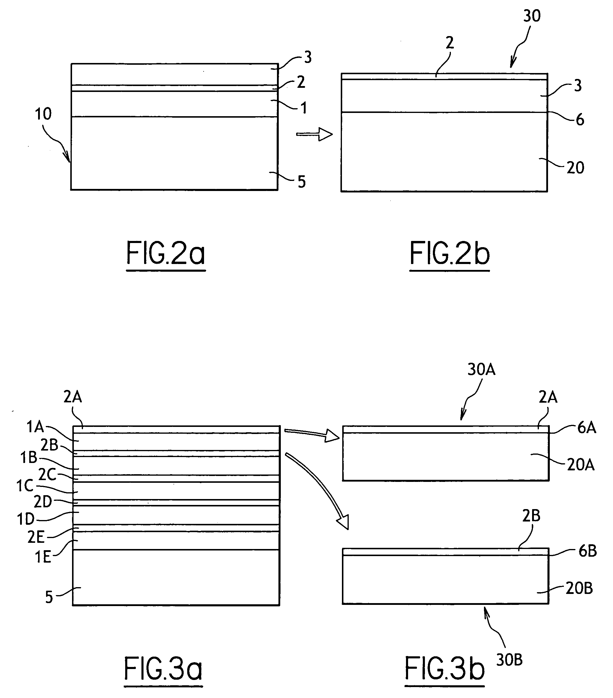
[0023] The present invention now provides, in a first preferred embodiment, a method of forming a structure comprising a removed layer of semiconductor material taken from a donor wafer, the donor wafer comprising, prior to removal, a first layer formed of Si1-xGex and a second layer formed of Si1-yGey on the first layer, where, as noted, x and y respectively are in the range of 0 to 1, and with x being different from y. This method preferably comprises the following steps in succession:

[0024] a) implanting atomic species to form a zone of weakness beneath the second layer and in the first layer;

[0025] b) bonding the donor wafer to a receiver wafer;

[0026] c) supplying energy to detach removed layers from the donor wafer at the zone of weakness;

[0027] d) conducting a RTA carried out at a temperature of about 1000° C. or more for a period not exceeding 5 minutes; and then

[0028] e) conducting selective etching of the remaining portion of the first layer as opposed to the second la...


PUM


Abstract

The invention relates to a method of forming a structure comprising a removed layer taken from a donor wafer, the donor wafer including a first layer formed of Si1-xGex and a second layer of Si1-yGey on the first layer, where x and y, respectively, are in the range of 0 to 1, with x being different from y. The method includes the steps of providing a donor wafer that includes a first layer of Si1-xGex and a second layer of Si1-yGey located on the first layer, with x and y respectively, being in the range of 0 to 1, and x being different than y; implanting atomic species into the donor wafer to form a zone of weakness in the first layer; bonding the donor wafer to a receiver wafer; detaching the second layer and a portion of the first layer from the donor wafer by supplying energy to bonded wafers sufficient to cause cleavage at the zone of weakness to form an intermediate structure thereof; conducting a rapid thermal anneal of the intermediate structure at a temperature of about 1000° C. or more for a period of time not exceeding 5 minutes; and removing any remaining portions of the first layer of the intermediate structure to provide a semiconductor structure comprising the second layer on the receiving wafer. Preferably, the remaining portions of the first layer are removed from the intermediate structure by selective etching.

Description

BACKGROUND OF THE INVENTION [0001] The present invention relates a method of forming a structure comprising a removed layer of semiconductor material taken from a donor wafer, the donor wafer comprising, prior to removal, a first layer formed of Si1-xGex and a layer of Si1-yGey on the first layer, with x and y respectively being in the range of 0 to 1 and x being different from y. This method comprises the following steps in succession: [0002] a) implanting atomic species to form a zone of weakness beneath the second layer; [0003] b) bonding the donor wafer to a receiver wafer; [0004] c) supplying thermal and / or mechanical energy to detach the removed layer from the donor wafer at the zone of weakness; [0005] d) treating the removed layer. [0006] The preferred type of layer removal uses a SMART-CUT® technique, a layer transfer method that is well known to a skilled person. One example of employing such a removal method is described in U.S. patent publication 2004 / 0053477 in which th...

Claims


Application Information

Patent Timeline
Patent Type & Authority Applications(United States)
IPC IPC(8): H01L21/30H01L21/46
CPCH01L21/26506H01L21/324H01L21/76254Y10S438/933
Inventor DAVAL, NICOLAS
Owner S O I TEC SILICON ON INSULATOR THECHNOLOGIES
Why Eureka
Try Eureka