
Area Sensor and Display Apparatus Provided with an Area Sensor

a technology of area sensor and display apparatus, which is applied in the field of area sensors, can solve problems such as inconsistencies in images

Inactive Publication Date: 2006-07-27
SEMICON ENERGY LAB CO LTD
View PDF35 Cites 23 Cited by
  • Summary
  • Abstract
  • Description
  • Claims
  • Application Information

AI Technical Summary

Benefits of technology

The present invention provides an area sensor that is small, thin, and light-weight, with no inconsistencies in lightness. The sensor uses a photodiode and an EL element as a photoelectric conversion device and a light source for reading an image. The sensor is controlled using thin film transistors and is capable of displaying an image without the need for a separate display. The sensor includes a matrix of photodiodes and EL elements, which ensures uniform lighting and eliminates the need for a separate backlight and light scattering plate. The sensor is also mechanically stronger and more robust without the need for precise adjustment of position. The technical effects of the present invention include small size, thinness, and lightness of the area sensor, as well as increased mechanical strength.

Problems solved by technology

In the above-mentioned area sensor, when light is not radiated uniformly to the subject from the backlight 2502, a read image may partially become light or dark, resulting in inconsistencies of the image.

Method used


Image

  • Area Sensor and Display Apparatus Provided with an Area Sensor
  • Area Sensor and Display Apparatus Provided with an Area Sensor
  • Area Sensor and Display Apparatus Provided with an Area Sensor

Examples


embodiment 1

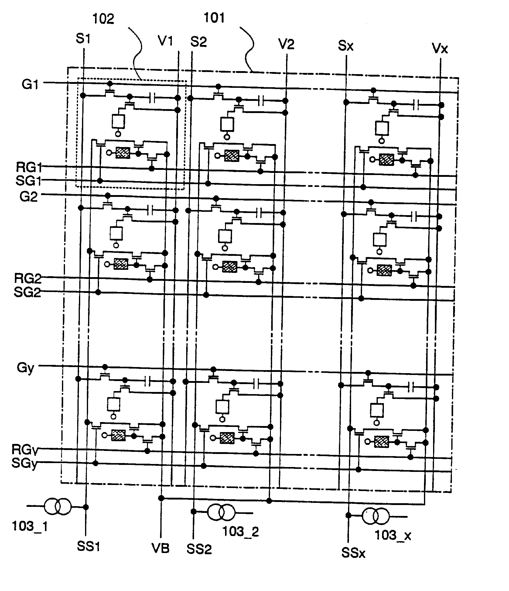
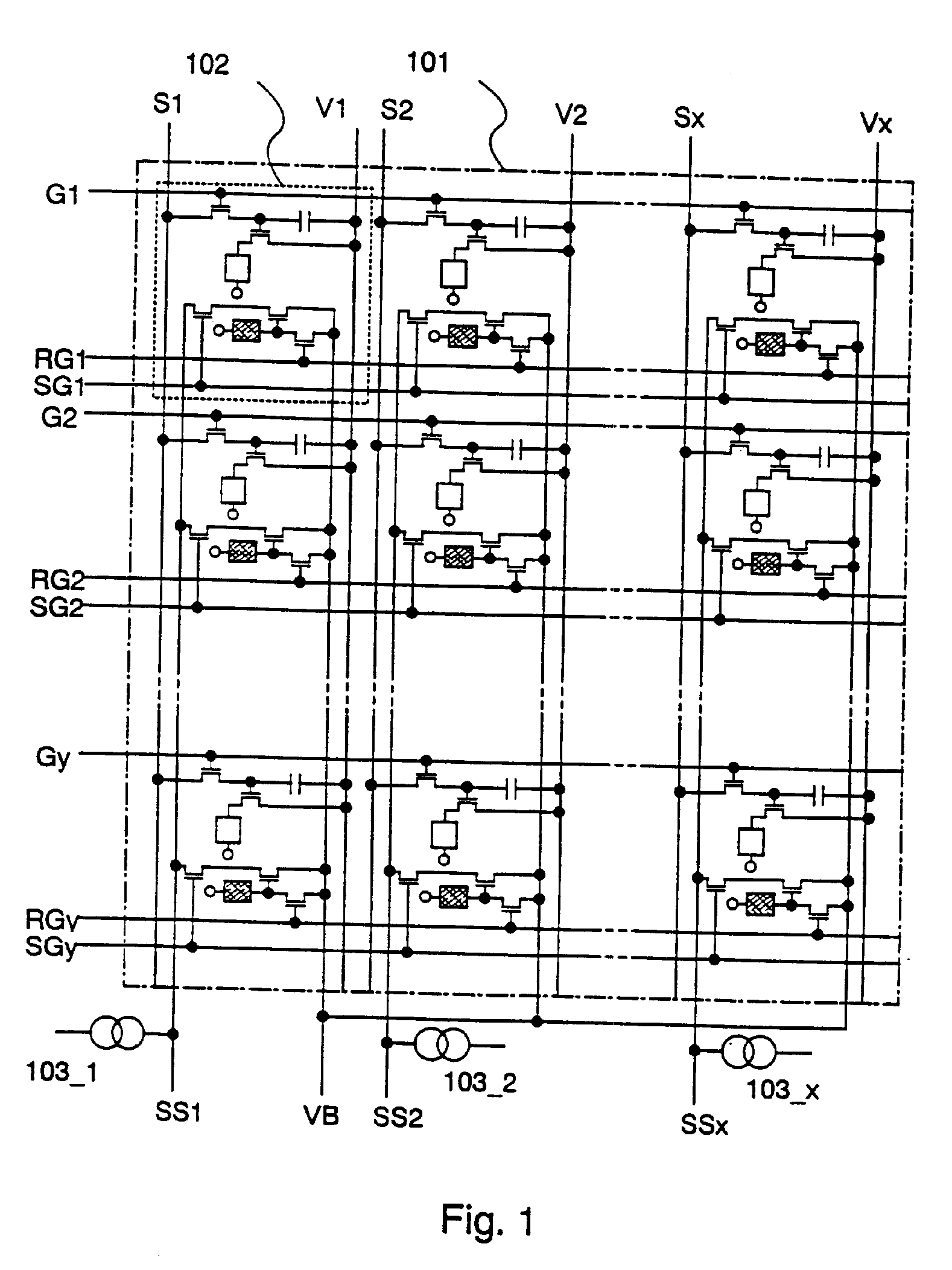
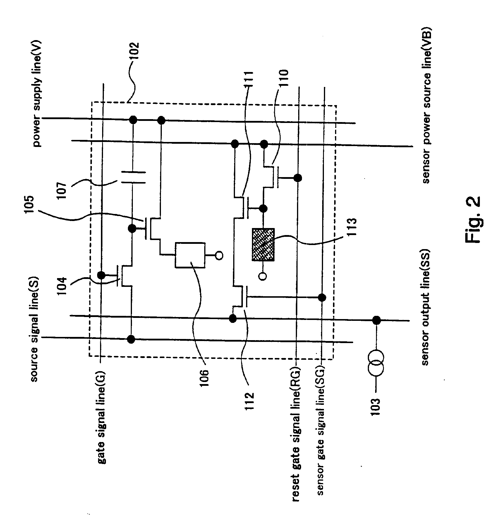
[0249] A method of driving the switching TFT 104 and the EL driving TFT 105, which control the operation of the EL element 106 shown in FIG. 2, is explained in Embodiment 1. Note that the structure of the sensor portion is the same as that of the embodiment mode, and therefore FIG. 1 and FIG. 2 are referenced.

[0250]FIG. 5 shows a top view of an area sensor of Embodiment 1. Reference numeral 120 denotes a source signal line driving circuit, reference numeral 122 denotes a gate signal line driving circuit, and both control the driving of the switching TFT 104 and the EL driving TFT 105. Further, reference numeral 121 denotes a sensor source signal line driving circuit, reference numeral 123 denotes a sensor gate signal line driving circuit, and both control the driving of the reset TFT 110, the buffer TFT 111, and the selection TFT 112. Note that the source signal line driving circuit 120, the gate signal line driving circuit 122, the sensor source signal line driving circuit 121, an...

embodiment 2

[0274] A method of driving the switching TFT 104 and the EL driving TFT 105 when displaying an image in the sensor portion 101 is explained in Embodiment 2. Note that the structure of the sensor portion is the same as the structure shown by the embodiment mode, and therefore FIG. 1 and FIG. 2 may be referenced.

[0275] A timing chart when performing display of an image in the sensor portion 101 in the area sensor of the present invention by a digital method is shown in FIG. 7.

[0276] First, one frame period F is divided into N subframe periods SF1 to SFN. The number of subframe periods in one frame period also increases as the number of gray scales increases. Note that, when the sensor portion of the area sensor displays an image, one frame period F denotes a period during which all pixels of the sensor portion display one image.

[0277] It is preferable that 60 or more frame periods be provided each second for the case of Embodiment 2. By setting the number of images displayed each s...

embodiment 3

[0295] The electric potential of the opposing electrodes are maintained at the same electric potential as that of the electric power source potential during the address period in Embodiments 1 and 2. Therefore, the EL elements do not emit light. However, the present invention is not limited to this structure. If an electric potential difference is always formed between the opposing electric potential and the electric power source potential, on an order at which the EL elements will emit light, when the electric power source potential is applied to the pixel electrodes, display may also be performed in the address period, similar to the display period.

[0296] However, when combining Embodiment 1, in which the EL elements are used as the light source of the area sensor, with Embodiment 3, it is important that the sensor frame period SF be contained within the frame period for an area sensor which reads in a single color image. Furthermore, it is important that the three subframe perio...


PUM


Abstract

An area sensor of the present invention has a function of displaying an image in a sensor portion by using light-emitting elements and a reading function using photoelectric conversion devices. Therefore, an image read in the sensor portion can be displayed thereon without separately providing an electronic display on the area sensor. Furthermore, a photoelectric conversion layer of a photodiode according to the present invention is made of an amorphous silicon film and an N-type semiconductor layer and a P-type semiconductor layer are made of a polycrystalline silicon film. The amorphous silicon film is formed to be thicker than the polycrystalline silicon film. As a result, the photodiode according to the present invention can receive more light.

Description

BACKGROUND OF THE INVENTION [0001] 1. Field of the Invention [0002] The present invention relates to an area sensor (semiconductor device) having an image sensor function and a display function. In particular, the present invention relates to an area sensor (semiconductor device) that has EL (electroluminescence) elements as a light source and is composed of photoelectric conversion devices provided on a flat surface (insulating surface) and a plurality of thin film transistors (TFTs) arranged in a matrix. [0003] 2. Description of the Related Art [0004] In recent years, a solid-state image sensing device is being used, which has diodes, CCDs, or the like for reading an electric signal having image information from a light signal having textural / graphic information, video information, and the like on a sheet of paper. Such a solid-state image sensing device is used for a scanner, a digital camera, and the like. [0005] The solid-state image sensing device having photoelectric conversi...

Claims


Application Information

Patent Timeline
Patent Type & Authority Applications(United States)
IPC IPC(8): H01L29/04H01L27/146H05B44/00H01L29/786H04N5/225H04N5/335H04N5/369H04N5/66H05B33/02H10K99/00
CPCH01L27/14623H01L27/14632H01L27/14643H01L27/14678H01L27/14687H01L27/3244H04N3/155H04N5/2251H01L27/15H01L27/3234Y02E10/549H01L27/14692H04N25/76H10K59/65H10K59/12H04N25/447H10K59/13H10K59/40H10K59/122H10K59/123H10K59/124H10K59/131H10K59/1213H10K59/1216H10K77/111H10K2102/311H01L29/78672G09G3/3258G09G3/3266G09G2300/0809G09G2310/0286G09G2310/0291G09G2320/0646
Inventor YAMAZAKI, SHUNPEIKOYAMA, JUNYONEZAWA, MASATOKIMURA, HAJIMEYAMAZAKI, YU
Owner SEMICON ENERGY LAB CO LTD
Learn More