Electronic image sensor

a sensor and electronic technology, applied in the field of cameras and camera components, can solve problems such as lowering the frame rate, and achieve the effects of avoiding prior art complications inherent, adequate exposure, and excellent image quality

Inactive Publication Date: 2006-07-27
E PHOCOS
View PDF13 Cites 133 Cited by
  • Summary
  • Abstract
  • Description
  • Claims
  • Application Information

AI Technical Summary

Benefits of technology

[0010] In this preferred embodiment charges generated in the pixels of each row of pixels are collected for a controlled period of time within the range of 65.2 microseconds to about 4.3 seconds. This charge collection time period is determined and set by a processor in the camera in which the sensor is utilized, within the above range, so as to achieve proper exposure (i.e. a desired quantity of charge collection in the pixels). Applicants refer to this charge collection time period as “shutter time” since it is equivalent to the time the shutter of a conventional (film type) camera is open. If the shutter time is less than the maximum per frame exposure time (about 33 milliseconds in this case) as it normally is, the frame rate will be determined using the factory set default value of row max (i.e. producing a frame rate of 30.2 fps with exposure times between 65.2 microseconds and about 33 milliseconds). If the shutter time is greater than the normal maximum per frame exposure time, a new calculated value of row-max is used to determine the frame rate so that the per frame exposure time is equal to the desired shutter time. With this technique the camera typically operates at the video rate of 30.2 Hz (with the camera controlling charge collection time periods to limit exposure) and at lower frame rates only when necessary to obtain desired exposures in low-light conditions. Thus, for video rate cameras using this sensor, desired exposures are automatically provided in low-light as well as good-light levels while avoiding prior art complications inherent in an adjustment of the master clock signal.
[0011] In preferred embodiments each pixel of the array includes light-sensing elements fabricated using CMOS techniques and CMOS or MOS based pixel circuits to store the charges and to convert the charges into electrical signals. In these preferred embodiments additional CMOS circuits in and / or on the same crystalline substrate are provided for parametric programming, chip timing, operation control and analog-to-digital data conversion circuits. A specific preferred embodiment is a CMOS sensor called the EPS 340C a 644×484 active pixel image array with 5 micron×5 micron pixels designed for operation at video frame rates up to about 30 frames per second when the input clock is at 12 MHz. The sensor has an integrated timing control that outputs a 10-bit digital video signal and synchronization clock signals. The sensor is designed as a versatile imaging sensor suitable for installation in a wide variety of electronic devices. Special features of the sensor permit sensor performance to be precisely controlled by software and electronics in the device in which the sensor is to be installed. The sensor is equipped with features permitting adjustable exposure time, and signal gain to accommodate various lighting conditions and sources. Specifically, sensor facilities permit camera controls to automatically reduced frame rates to permit adequate exposures times if light levels detected by the camera are below predetermined values. In an example embodiment where the nominal video rate is about 25 frames per second with an input clock at 10 MHz, the sensor is programmed to automatically reduce frame rates as necessary to maintain adequate exposure. The EPS304C achieves excellent image quality. The sensor has low light sensing capability, high pixel dynamic range and uses a special scheme for column fixed pattern noise reduction. The EPS304C maintains a consistent optical black level with its automated offset compensation circuitry so that variation in sensor output from sensor to sensor is minimal. Therefore, the sensor is useful as a component part of low-cost mass-produced electronic consumer products such as cell phones and digital cameras. The EPS304C can operate from a single 3.3V DC bias voltage or with 3.3V and 2.5V dual supplies.

Problems solved by technology

(There is an obvious compromise of lowering of the frame rate in conditions of very low light levels, but in most cases this is preferable to inadequate exposure.)

Method used


Image

  • Electronic image sensor
  • Electronic image sensor
  • Electronic image sensor

Examples


Embodiment Construction

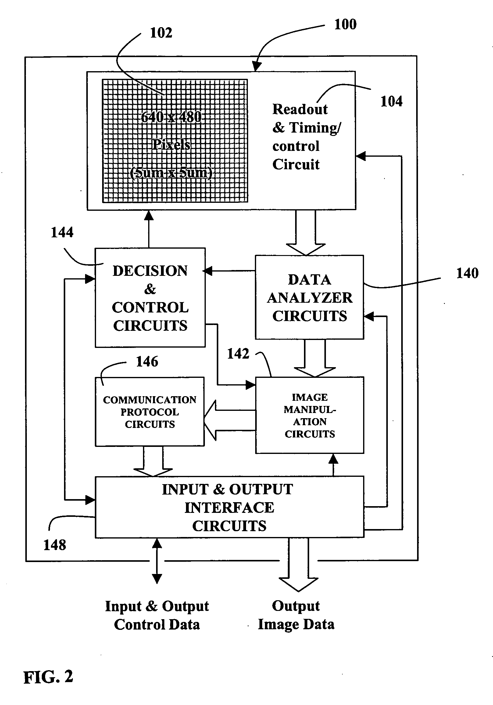
[0009] In a preferred embodiment the predetermined normal video frame rate is determined by a master clock frequency signal (at for example 12 MHz) divided by the product of two numbers representing: (1) the maximum number of rows of pixels, row-max and (2) the maximum number of columns of pixels, col-max. Default values of these two numbers are preferably factory set (for example, at 508 for row-max and 782 for col-max) by the sensor fabricator providing a frame rate of 30.2 Hz. With this frame rate the predetermined normal maximum per frame exposure time is about 33 milliseconds. However, in this embodiment, provisions are made for a calculation of new row max values that are used instead of the factory set value of row-max whenever necessary to reduce the frame rate to achieve desired exposures in low light levels.

[0010] In this preferred embodiment charges generated in the pixels of each row of pixels are collected for a controlled period of time within the range of 65.2 micros...


PUM


Abstract

An electronic imaging sensor. The sensor includes an array of photo-sensing pixel elements for producing image frames. Each pixel element defines a photo-sensing region and includes a charge collecting element for collecting electrical charges produced in the photo-sensing region, and a charge storage element for the storage of the collected charges. The sensor also includes charge sensing elements for sensing the collected charges, and charge-to-signal conversion elements. The sensor also includes timing elements for controlling the pixel circuits to produce image frames at a predetermined normal frame rate based on a master clock signal (such as 12 MHz or 10 MHz). This predetermined normal frame rate which may be a video rate (such as about 30 frames per second or 25 frames per second) establishes a normal maximum per frame exposure time. The sensor includes circuits (based on prior art techniques) for adjusting the per frame exposure time (normally based on ambient light levels) and novel frame rate adjusting features for reducing the frame rate below the predetermined normal frame rate, without changing the master clock signal, to permit per frame exposure times above the normal maximum exposure time. This permits good exposures even in very low light levels. (There is an obvious compromise of lowering of the frame rate in conditions of very low light levels, but in most cases this is preferable to inadequate exposure.) These adjustments can be automatic or manual.

Description

CROSS REFERENCE TO RELATED APPLICATIONS [0001] This application is a continuation in part of U.S. patent application Ser. No. 10 / 921,387, filed Aug. 18, 2004 which was a continuation in part of Ser. No. 10 / 229,953 filed Aug. 27, 2002; Ser. No. 10 / 229,954 filed Aug. 27, 2002, now U.S. Pat. No. 6,791,130; Ser. No. 10 / 229,955 filed Aug. 27, 2002; Ser. No. 10 / 229,956 filed Aug. 27, 2002, now U.S. Pat. No. 6,798,033; Ser. No. 10 / 648,129 filed Aug. 26, 2003, now U.S. Pat. No. 6,809,358; and Ser. No. 10 / 746,529 filed Dec. 23, 2003, all incorporated herein by reference. Ser. No. 10 / 648,129 was a continuation in part of Ser. No. 10 / 672,637 filed Feb. 5, 2002 now U.S. Pat. No. 6,370,914 which is also incorporated herein by reference.FIELD OF THE INVENTION [0002] The present invention relates to cameras and camera components and in particular CMOS image sensors and to cameras with CMOS image sensors. BACKGROUND OF THE INVENTION [0003] Electronic cameras comprise imaging components to produce a...

Claims


Application Information

Patent Timeline
Patent Type & Authority Applications(United States)
IPC IPC(8): H04N3/14H04N5/335H04N5/353H04N5/365H04N5/372H04N9/07H04N9/73
CPCH01L27/14632H04N5/2257H04N5/2353H04N5/353H04N5/374H04N5/3765H04N23/57H04N23/73H04N25/53H04N25/745H04N25/76
Inventor HSIEH, TZU-CHIANGCHAO, CALVIN
Owner E PHOCOS
Why Eureka
Try Eureka