Polishing apparatus and polishing method

a polishing apparatus and polishing technology, applied in the direction of grinding machine components, manufacturing tools, lapping machines, etc., can solve the problems of short circuit, large step height on the surface of semiconductor devices, and complicated structure of semiconductor elements, so as to prevent the reduction of manufacturing yield and increase the manufacturing cost

Active Publication Date: 2006-07-27
EBARA CORP
View PDF11 Cites 36 Cited by
  • Summary
  • Abstract
  • Description
  • Claims
  • Application Information

AI Technical Summary

Benefits of technology

[0012] The present invention has been made in view of the above drawbacks. It is, therefore, an object of the present invention to provide a polishing apparatus and a substrate polishing method which can polish a substrate with accuracy so as to have a desired film thickness, can prevent a manufacturing yield from being lowered by excessively polishing, and can prevent manufacturing cost from being increased by reworking processes.

Problems solved by technology

In recent years, semiconductor devices have become more integrated, and structures of semiconductor elements have become more complicated.
Accordingly, irregularities on a surface of a semiconductor device are increased, so that step heights on the surface of the semiconductor device tend to be large.
When the number of irregularities is increased on a surface of a semiconductor device, the following problems arise.
Further, an open circuit may be caused by disconnection of interconnects, or a short circuit may be caused by insufficient insulation between interconnect layers.
As a result, good products cannot be obtained, and the yield tends to be lowered.
Further, even if a semiconductor device initially works normally, reliability of the semiconductor device is lowered after a long-term use.
Therefore, if the irregularities of the surface of the semiconductor device are increased, then it becomes problematically difficult to form a fine pattern itself on the semiconductor device.
However, in the polishing apparatus, a polishing rate largely depends upon surface conditions of a polishing pad, conditions of a pad conditioner for conditioning a surface of the polishing pad, a composition and temperature of a polishing liquid, a temperature and pressure of a deposition process, a non-uniformity of properties of films due to variations of materials, and variations in polishing temperature.
Thus, a polishing rate is not necessarily maintained stable at an average polishing rate.

Method used


Image

  • Polishing apparatus and polishing method
  • Polishing apparatus and polishing method
  • Polishing apparatus and polishing method

Examples


first embodiment

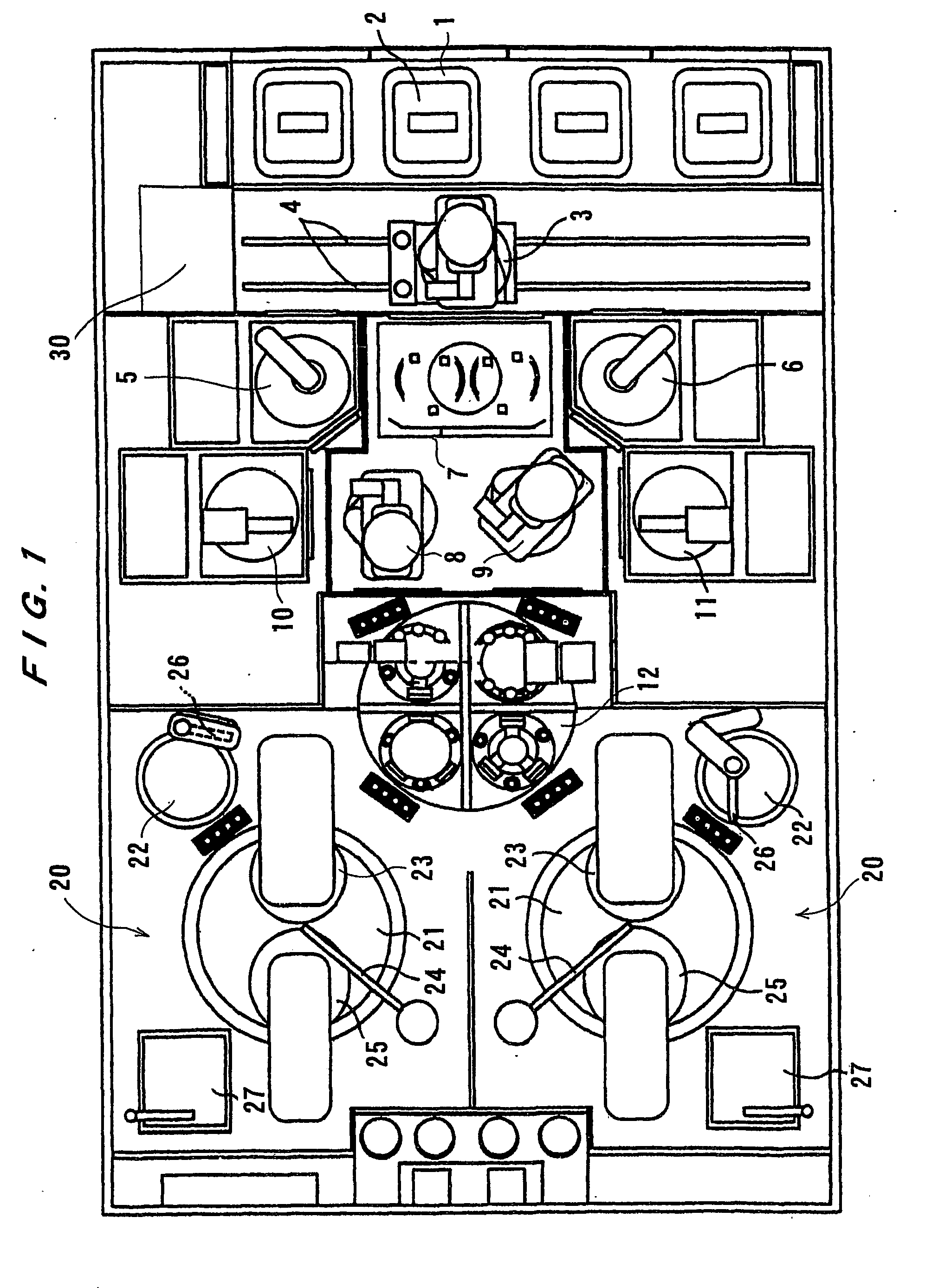
[0049]FIG. 1 is a plan view showing a whole arrangement of a polishing apparatus according to the present invention. As shown in FIG. 1, the polishing apparatus has four load / unload stages 1 each for receiving a cassette 2 which accommodates (or stocks) a plurality of substrates such as semiconductor wafers. The polishing apparatus also has a transfer robot 3 provided on rails 4 so that the transfer robot 3 can move along the rails 4 to access respective cassettes 2 at respective load / unload stages 1. The polishing apparatus also has two cleaning units 5 and 6 disposed at an opposite side of the rails 4 to the load / unload stages 1, and a substrate station 7 disposed between the two cleaning units 5 and 6 at a position accessible by the transfer robot 3. These cleaning units 5 and 6 are used for cleaning and drying a substrate after polishing. The cleaning units 5 and 6 are disposed at positions accessible by hands of the transfer robot 3.

[0050] The polishing apparatus includes a tra...

second embodiment

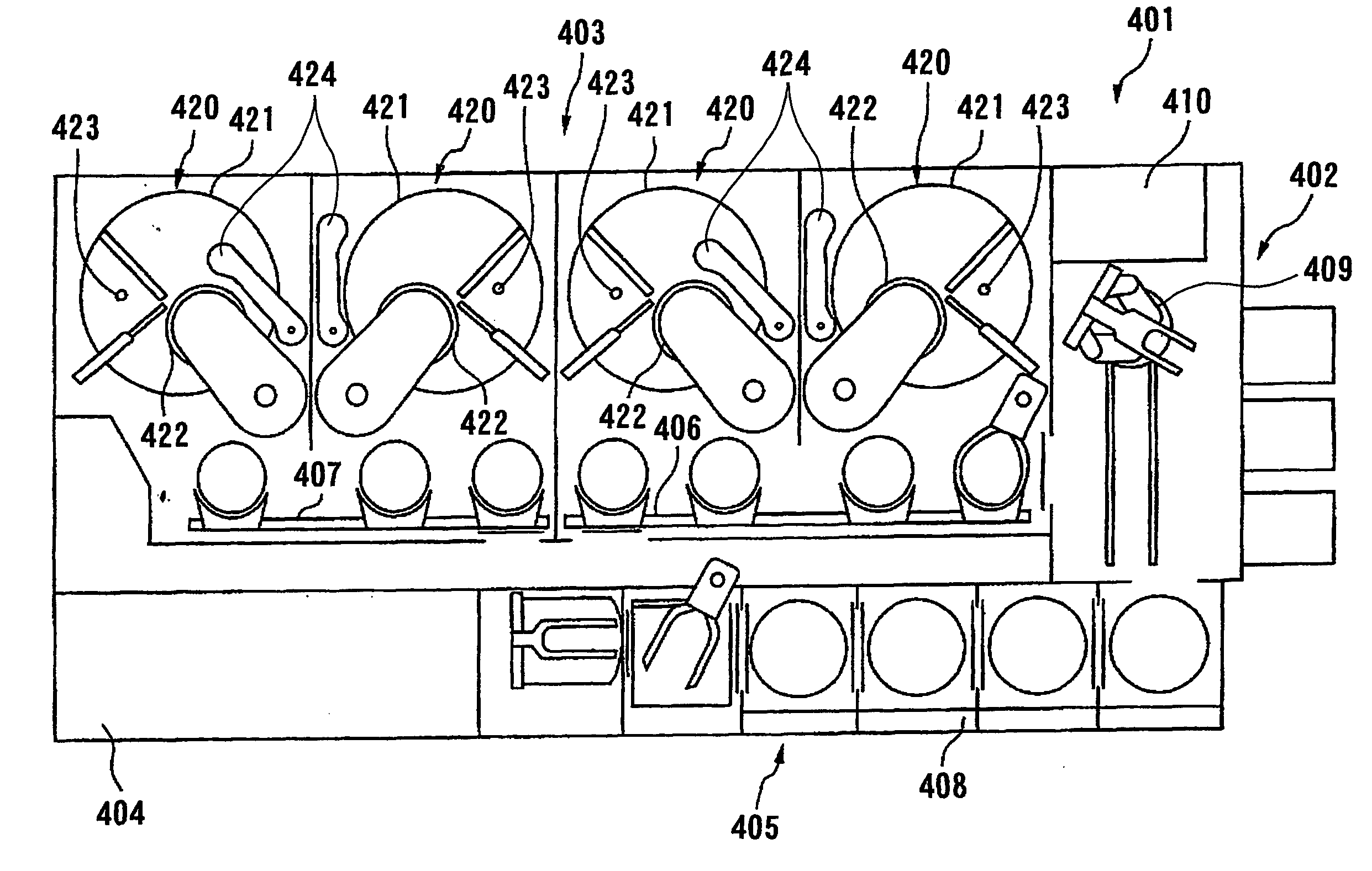
[0099]FIG. 8 is a plan view showing a whole arrangement of a polishing apparatus according to the present invention. As shown in FIG. 8, the polishing apparatus 401 has a loading / unloading section 402, a polishing section 403, a controller 404, a cleaning section 405, an in-line film thickness measurement device 410, and a transferring section including two linear transporters 406 and 407, a transfer unit 408, and a transfer robot 409. The polishing section 403 includes four polishing units 420. Each of the polishing units 420 includes a polishing table 421, a top ring 422, an in-situ film thickness measurement device 423 provided in the polishing table 421, and a dresser 424. The in-line film thickness measurement device 410 is located substantially outside of the polishing tables 421.

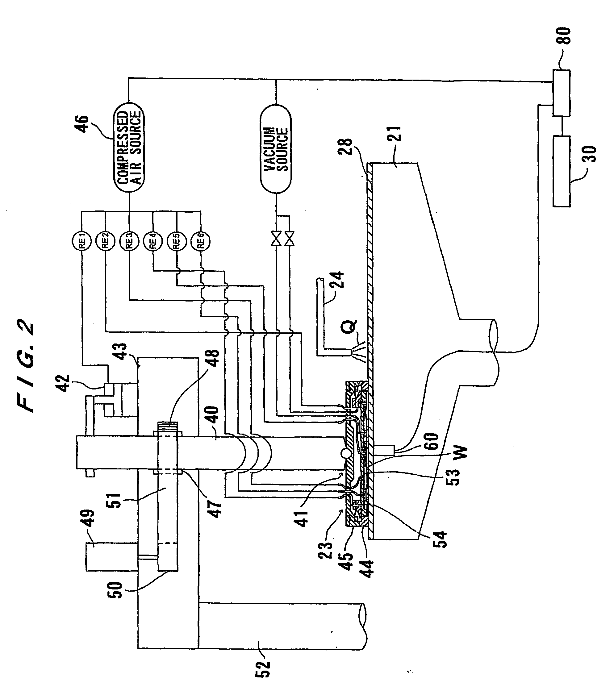
[0100]FIG. 9 is a cross-sectional view showing a portion of the polishing unit 420 shown in FIG. 8. Each of the other polishing units 420 has the same structure. The polishing unit 420 has the polishi...


PUM

PropertyMeasurementUnit
pressureaaaaaaaaaa
thicknessaaaaaaaaaa
thicknessaaaaaaaaaa

Abstract

A polishing apparatus has a polishing section (302) configured to polish a substrate and a measurement section (307) configured to measure a thickness of a film formed on the substrate. The polishing apparatus also has an interface (310) configured to input a desired thickness of a film formed on a substrate to be polished and a storage device (308a) configured to store polishing rate data on at least one past substrate therein. The polishing apparatus includes an arithmetic unit (308b) operable to calculate a polishing rate and an optimal polishing time based on the polishing rate data and the desired thickness by using a weighted average method which weights the polishing rate data on a lately polished substrate.

Description

TECHNICAL FIELD [0001] The present invention relates to a polishing apparatus and a polishing method, and more particularly to a polishing apparatus and a polishing method for polishing a substrate such as a semiconductor wafer to a flat mirror finish. BACKGROUND ART [0002] In recent years, semiconductor devices have become more integrated, and structures of semiconductor elements have become more complicated. Further, the number of layers in multilayer interconnects used for a logical system has been increased. Accordingly, irregularities on a surface of a semiconductor device are increased, so that step heights on the surface of the semiconductor device tend to be large. This is because, in a manufacturing process of a semiconductor device, a thin film is formed on a semiconductor device, then micromachining processes, such as patterning or forming holes, are performed on the semiconductor device, and these processes are repeated to form subsequent thin films on the semiconductor ...

Claims


Application Information

Patent Timeline
Patent Type & Authority Applications(United States)
IPC IPC(8): B24B49/00H01L21/461B24B51/00B24B37/04B24B49/03H01L21/321
CPCB24B37/042H01L21/3212B24B49/03
Inventor SASAKI, TATSUYAYAMADA, NAOSHIKATSUMATA, YOSHIFUMISHIMIZU, NOBURUTSUNO, SEIRYOMITSUYA, TAKASHI
Owner EBARA CORP
Why Eureka
Try Eureka