Organic light emitting device and method of manufacturing the same

a technology of light-emitting devices and organic materials, which is applied in the direction of discharge tubes/lamp details, discharge tubes luminescnet screens, other domestic articles, etc., can solve the problems of insufficient development of proper deposition equipments for producing large-scale screens, inefficient use, and increased manufacturing costs. achieve the effect of long life and high efficiency

Active Publication Date: 2006-08-03
SAMSUNG DISPLAY CO LTD
View PDF12 Cites 7 Cited by
  • Summary
  • Abstract
  • Description
  • Claims
  • Application Information

AI Technical Summary

Benefits of technology

[0018] The organic light emitting device includes a multiple emissive layer having a greater no−ne parameter than that of a single-coated emissive layer so that long lifetime and high efficiency can be obtained. The organic light emitting device can be manufactured using a method of manufacturing an organic light emitting device according to the present invention.

Problems solved by technology

In this case, however, materials for forming these layers are inefficiently used, and thus, the manufacturing costs increase.
In addition, proper deposition equipments for producing large screens have not been developed.
Accordingly, when an organic layer of a PLED is formed using this method, a manufacturing time is long and manufacturing costs are high.
As described above, when an organic layer, in particular, an emissive layer interposed between first and second electrodes is formed using conventional methods, characteristics of the organic layer do not meet a required standard.

Method used


Image

  • Organic light emitting device and method of manufacturing the same
  • Organic light emitting device and method of manufacturing the same
  • Organic light emitting device and method of manufacturing the same

Examples


example 1

Measurement Example 1

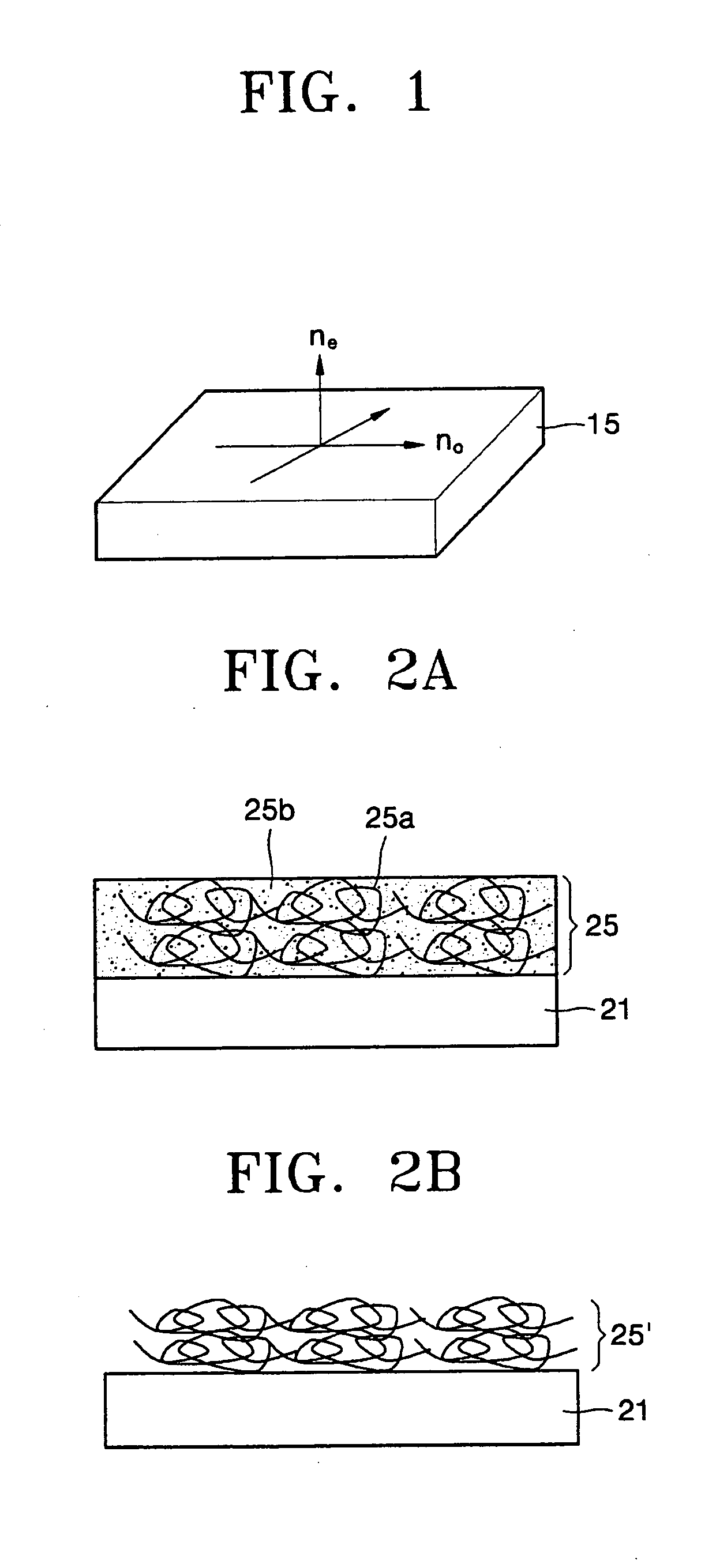
no and no−ne of Samples 1, A and B

[0121] no and no−ne parameters of Samples 1, A and B were shown in FIGS. 7 and 8, respectively. no and no−ne parameters of Samples 1, A and B was measured using ellipsometer (Variable Angle Spectroscopic Eilipsomer (VASE) VD-250, obtained from J. A. Woollam Co.). The results were analyzed using WVASE 32 Version 3.45 (obtained from J. A. Woollam. Co. Inc). In general, an ellipsometer used for ellipsometry includes a lamp that is a white light source, a polarizing device that polarizes light, a monochrometer that separates a short-wavelength light form the white light source, and a detector that decodes a signal.

[0122]FIG. 7 illustrates no obtained through spectroscopic ellipsometry at 2.58 eV. Referring to FIG. 7, no of Sample A is about 1.680, no of Sample B is about 1.698, and no of Sample 1 is about 1.7025. That is, no of Sample 1 was greater than no of Samples A and B by about 0.005. As a result, it was confirmed that Sampl...

example 2

[0126] 15 Ω / cm2 (1200 Å) ITO glass substrate (obtained from Corning Co.) was cut to a size of 50 mm×50 mm×0.7 mm, washed in pure water using an ultrasonic wave for 5 minutes, washed in isopropyl alcohol using an ultrasonic wave for 5 minutes, and washed using ultra violet (UV) light and ozone for 30 minutes. PEDOT / PSS (Baytron P AI4083, obtained from Bayer Co.) was coated to a thickness of 50 nm on the substrate at 2,000 rpm and then heat-treated at 200° C. for 10 min to form a hole injection layer.

[0127] PFB (a hole transporting material obtained from Dow Chemical Co.) was spin coated on the hole injection layer to form a 10 nm-thick hole transport layer, and then heat-treated at 220° C. for 1 hour.

[0128] Some of a mixture of 1.4 wt % of a spirofluorene-based blue emissive material having a molecular weight of 0.3 million dissolved in xylene was applied to the hole transport layer using a micro pipette, and spin coated thereon to a thickness of 85 nm to form a single-coated layer...

example 4

Measurement Example 4

[0132] A 15 Ω / cm2 (1200 Å) ITO glass substrate (obtained from Corning Co.) was cut to a size of 50 mm×50 mm×0.7 mm, washed in pure water using an ultrasonic wave for 5 minutes, washed in isopropyl alcohol using an ultrasonic wave for 5 minutes, and washed using ultra violet (UV) light and ozone for 30 minutes. PEDOT / PSS (Baytron P AI4083, obtained from Bayer Co.) was coated to a thickness of 50 nm on the substrate at 2,000 rpm and then heat-treated at 200° C. for 10 min to form a hole injection layer.

[0133] PFB (a hole transporting material obtained from Dow Chemical Co.) was spin coated on the hole injection layer and heat treated at 220° C. for 1 hour in a nitrogen atmosphere to form a 10 nm-thick hole transport layer.

[0134] Some of a mixture of 0.4 wt % of a spirofluorene-based blue emissive material having a molecular weight of 1.5 million dissolved in xylene was applied to the hole transport layer using a micro pipette, and spin coated thereon to a thickn...


PUM

PropertyMeasurementUnit
energy band gapaaaaaaaaaa

Abstract

An organic light emitting device and a method of manufacturing the same, the organic light emitting device includes a first electrode, a second electrode, and an organic layer that has at least a multi-coated emissive layer and which is interposed between the first and second electrodes. The multi-coated emissive layer is a single layer composed of a neutral emissive material and an no−ne parameter of the emissive layer is greater than an no−ne parameter of a single-coated layer. The organic light emitting device has a longer lifetime and high efficiency.

Description

CROSS-REFERENCE TO RELATED PATENT APPLICATIONS AND CLAIM OF PRIORITY [0001] This application claims the benefit of Korean Patent Application No. 10-2005-0010178, filed on Feb. 3, 2005, in the Korean Intellectual Property Office, the disclosure of which is incorporated herein in its entirety by reference. BACKGROUND OF THE INVENTION [0002] 1. Field of the Invention [0003] The present invention relates to an organic light emitting device and a method of manufacturing the same, and more particularly, to an organic light emitting device including an emissive layer, of which an no−ne parameter is greater than an no−ne parameter of a single-coated emissive layer where no is an ordinary refractive index and ne is a extraordinary refractive index and a method of manufacturing the same. [0004] 2. Description of the Related Art [0005] Organic light emitting devices (OLEDs) are self-emissive devices that emit light by combination of electron and holes in a fluorescent or phosphorescent organic...

Claims


Application Information

Patent Timeline
Patent Type & Authority Applications(United States)
IPC IPC(8): H05B33/00H01J1/62
CPCC09K11/06C09K2211/1416C09K2211/1425C09K2211/1458H01L51/0037H01L51/0039H01L51/5012H01L51/5036H05B33/14H10K85/115H10K85/1135H10K50/125H10K50/11B29C53/562B29C53/8016B29C53/845B29L2023/22B29K2105/26B29K2023/06
Inventor LEE, TAE-WOOKIM, SANG-YEOLKIM, MU-GYEOMKIM, YU-JINPU, LYONG-SUNPARK, JONG-JINPARK, SANG-HOONKANG, IN-NAM
Owner SAMSUNG DISPLAY CO LTD
Why Eureka
Try Eureka