Phosphorescent organic electroluminescence devices

a phosphorescent organic and electroluminescent technology, applied in the direction of luminescent compositions, organic chemistry, chemistry apparatus and processes, etc., can solve the problems of reducing device efficiency and high phosphorescent dye doping concentration, and achieves the effect of improving device stability, reducing the doping concentration of phosphorescent dye, and increasing device efficiency

Inactive Publication Date: 2018-12-27
KUNSHAN GO VISIONOX OPTO ELECTRONICS CO LTD +1
View PDF2 Cites 6 Cited by
  • Summary
  • Abstract
  • Description
  • Claims
  • Application Information

AI Technical Summary

Benefits of technology

[0019]The present invention has the following advantages:
[0020]In the phosphorescent organic electroluminescence device of the present invention, the luminescent layer is a double-layer structure and the exciplex is formed on the interface of the hole transport material layer and the electron transport material layer, the exciplex is a TADF exciplex having a thermally activated delayed fluorescence effect, and the triplet state energy of the TADF exciplex is transferred to the singlet state energy by reverse intersystem crossing and then transferred to the triplet state energy of the dopant dye; so that the triplet state energy of the host material and dopant dye in the device can be fully utilized, thereby increasing the device efficiency; and the energy transfer process and luminescent process of thermally activated delayed fluorescence occur in different materials (named as thermally activated sensitization process), so that the problem of significant roll-off under high luminance conditions can be effectively solved, thereby further improving the stability of the device.
[0021]In the phosphorescent organic electroluminescence device of the present invention, the luminescent layer utilizes the exciplex to reduce the doping concentration of the phosphorescent dye and also maintain long lifetime and high efficiency.

Problems solved by technology

In a phosphorescent device in which a conventional host exists, energy is transferred from the host at triplet state to a phosphorescent guest at triplet state by short-range Dexter energy transfer, resulting in a higher doping concentration (10 wt %-30 wt %) of the phosphorescent material; although the high doping concentration may reduce the distance between the host and guest and promote complete transfer of energy, the excessive high doping concentration may cause the decrease of device efficiency, also, as the phosphorescent material is made of a noble metal, the high phosphorescent dye doping concentration may increase the cost.

Method used


Image

  • Phosphorescent organic electroluminescence devices
  • Phosphorescent organic electroluminescence devices
  • Phosphorescent organic electroluminescence devices

Examples


example 1

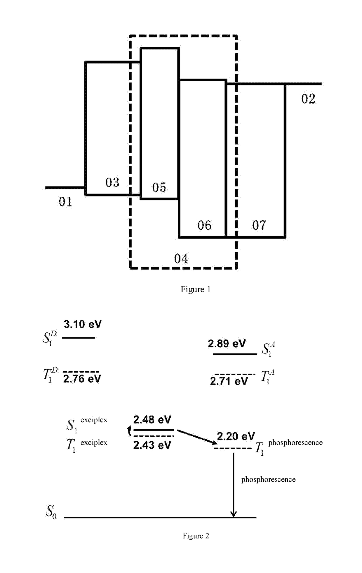
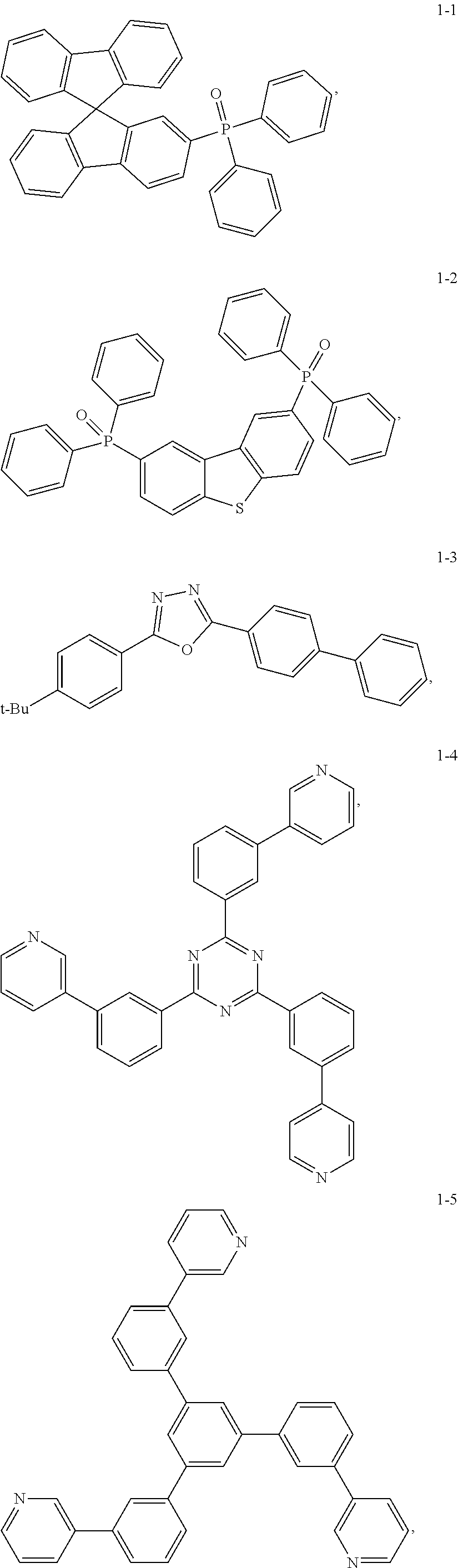
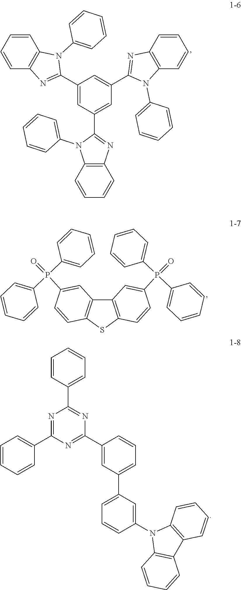
[0053]In this example, luminescent devices in which a hole transport material layer 05 and an electron transport material layer 06 in a luminescent layer have different thicknesses are manufactured, and these devices have a structure shown as FIG. 1. In the luminescent layer, the hole transport material layer 05 consists of a host material compound (2-5) TCTA, and the electron transport material layer 06 consists of a host material compound (1-8) CzTrz and a phosphorescent dye PO-01. The difference in LUMO energy level between the host compound (2-5) TCTA and the acceptor host compound (1-8) CzTrz is more than 0.3 eV, and the difference in HOMO energy is more than 0.2 eV; and the first singlet state energy level of the exciplex is higher than the first triplet state energy level of the phosphorescent dye. The phosphorescent dye PO-01 accounts for 3 wt % of the luminescent layer.

[0054]The device of this example has the following structure.

[0055]ITO (150 nm) / NPB (40 nm) / hole transport...

example 2

[0070]The device of this example has the following structure.

[0071]ITO (150 nm) / NPB (40 nm) / TCTA (10 nm) / CzTrz+1-10 wt % phosphorescent dye PO-01(30 nm) / Bphen (20 nm) / LiF (0.5 nm) / Al (150 nm)

[0072]The phosphorescent dye PO-01 accounts for 1-10 wt % of the luminescent layer. In this example, different doping concentrations of phosphorescent dye were applied in the luminescent layer for experiments, and the results were shown in Table 2.

TABLE 2ExternalLuminousquantumLifetimeefficiencyLuminanceefficiencyT97Luminescent layer(cd / A)(cd / m2)(%)(hrs)TCTA (10) / CzTrz:58100014.14351 wt % PO-01 (30 nm)TCTA (10) / CzTrz:61100014.74622 wt % PO-01 (30 nm)TCTA (10) / CzTrz:64100016.14803 wt % PO-01 (30 nm)TCTA (10) / CzTrz:57100014.64715 wt % PO-01 (30 nm)TCTA (10) / CzTrz:54100012.944310 wt %PO-01 (30 nm)

[0073]It can be seen from Table 2 that when the doping concentration of the phosphorescent dye in the luminescent layer is 3 wt %, both the external quantum efficiency and the lifetime of the OLED device a...

example 3

[0074]In order to evaluate the influence of the host material on the performance of the organic electroluminescence device of the present invention, an organic electroluminescence device was manufactured by the same method as Example 1, having the following structure:

[0075]ITO (150 nm) / NPB (40 nm) / hole transport material layer (material having hole transport capability) (10 nm) / electron transport material layer (material having electron transport capability +3 wt % phosphorescent dye) (30 nm) / Bphen (20nm) / LiF (0.5nm) / Al (150 nm)

[0076]The performance of the organic electroluminescence device is shown in Table 3 below:

TABLE 3LuminousExternal quantumLifetimeHole transportElectron transportefficiencyLuminanceefficiencyT97Devicematerial layermaterial layer(cd / A)(cd / m2)(%)(hrs)OLED1compoundcompound (1-3) +23100018390(2-7)phosphorescentdye Ir(piq)3OLED2compoundcompound (1-7) +20100016348(2-7)phosphorescentdye Ir(DBQ)2(acac)OLED3.compoundcompound (1-1) +67100017390(2-5)phosphorescentdye Ir(...


PUM


Abstract

The present invention discloses a phosphorescent organic electroluminescence device including a hole transport layer, a luminescent layer and an electron transport layer, which are successively laminated. The luminescent layer has a double-layer structure comprising a hole transport material layer and an electron transport material layer. The hole transport material layer is arranged between the hole transport layer and the electron transport material layer. The electron transport material layer is arranged between the hole transport material layer and the electron transport layer. An exciplex is formed on the interface of contact between the hole transport material layer and the electron transport material layer. The hole transport material layer includes a host material, the host material being a material having hole transport capability; and the electron transport material layer includes a host material and a phosphorescent dye doped in the host material, the host material being a material having electron transport capability.

Description

TECHNICAL FIELD[0001]The present invention belongs to the field of organic electroluminescence devices, and specifically relates to a phosphorescent organic electroluminescence device.BACKGROUND ART[0002]Organic electroluminescence devices have attracted extensive attention due to their features of thinness, large area, full curing and flexibility, and their potential in solid-state lighting sources and liquid crystal backlights has become a focus of research.[0003]As early as in 1950s, Bernanose. A et al. began the research on organic electroluminescence devices (OLEDs). Anthracene single crystal wafer was adopted as the original research materials. Because of large thickness of the single crystal wafer, the driving voltage required is very high. Until 1987, C. W. Tang and Vanslyke from Eastman Kodak Company proposed an organic small molecule electroluminescence device having the structure ITO / Diamine / Alq3 / Mg:Ag. It was reported that when this device worked at a working voltage of ...

Claims


Application Information

Patent Timeline
Patent Type & Authority Applications(United States)
IPC IPC(8): H01L51/50H01L51/00
CPCH01L51/5096H01L51/005H01L51/0081H01L51/0085H01L51/5016H01L51/5052H10K85/00H10K50/00H10K50/11H10K2101/40H10K30/865H10K50/80H10K85/631H10K85/633H10K85/654H10K85/6565H10K85/6576H10K85/6572H10K50/165H10K2101/90C07D333/76C07D401/14C07D403/14C09K11/06H10K50/125H10K50/15H10K2101/27H10K2101/30H10K50/18H10K85/60H10K85/324H10K85/342H10K2101/10
Inventor DUAN, LIANZHANG, DONGDONGLIU, SONGZHAO, FEI
Owner KUNSHAN GO VISIONOX OPTO ELECTRONICS CO LTD
Why Eureka
Try Eureka