
Wiring board and method for fabricating the same

Active Publication Date: 2006-08-10
FUJITSU LTD
View PDF3 Cites 22 Cited by
  • Summary
  • Abstract
  • Description
  • Claims
  • Application Information

AI Technical Summary

Benefits of technology

[0010] An object of the present invention is to provide a wiring board having high reliability and a method for fabricating the same, which ensure the insulation between a conductive core material and wiring patterns.
[0014] According to the present invention, the insulation layer is formed on the inside wall of the through-hole in the conductive core material, covering burrs, whereby the conductive core material and the wirings can be surely insulated from each other. Accordingly, the present invention can provide a wiring board of high reliability.
[0015] According to the present invention, the insulation layer is formed on-the inside wall of the through-hole in the conductive core material, covering burrs with the metal layer formed therebetween, whereby the insulation layer is formed with higher adhesion. Accordingly, the conductive core material and the wirings can be further surely insulated from each other. Accordingly, the present invention can provide a wiring board of high reliability.

Problems solved by technology

Thus, the use of epoxy resin makes it difficult to sufficiently decrease the thermal expansion coefficient of the printed circuit board.
However, many of these low thermal expansion coefficient materials are conductive, as is not the glass epoxy resin board.
In the step of filling the through-holes by the conventional printing, the fillers, such as epoxy resin, etc., often become short.

Method used


Image

  • Wiring board and method for fabricating the same
  • Wiring board and method for fabricating the same
  • Wiring board and method for fabricating the same

Examples


first embodiment

A First Embodiment

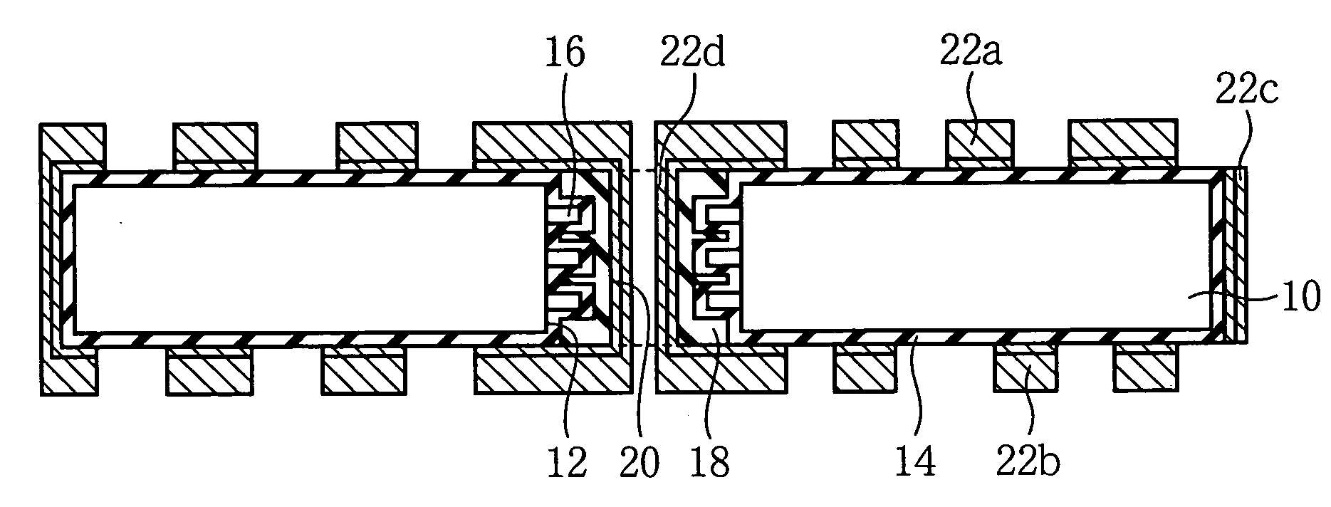
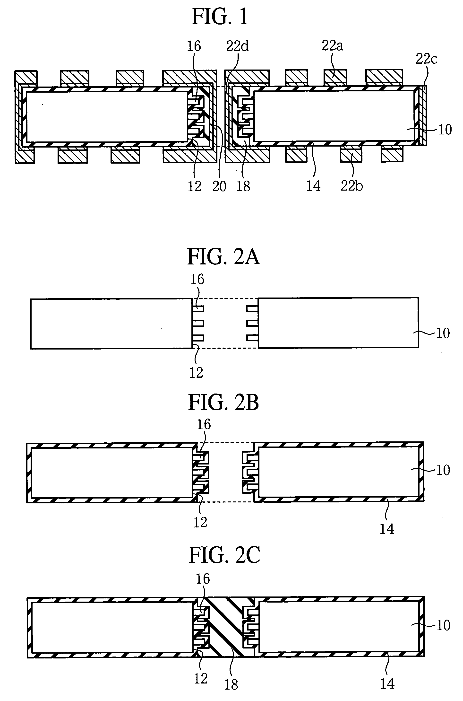
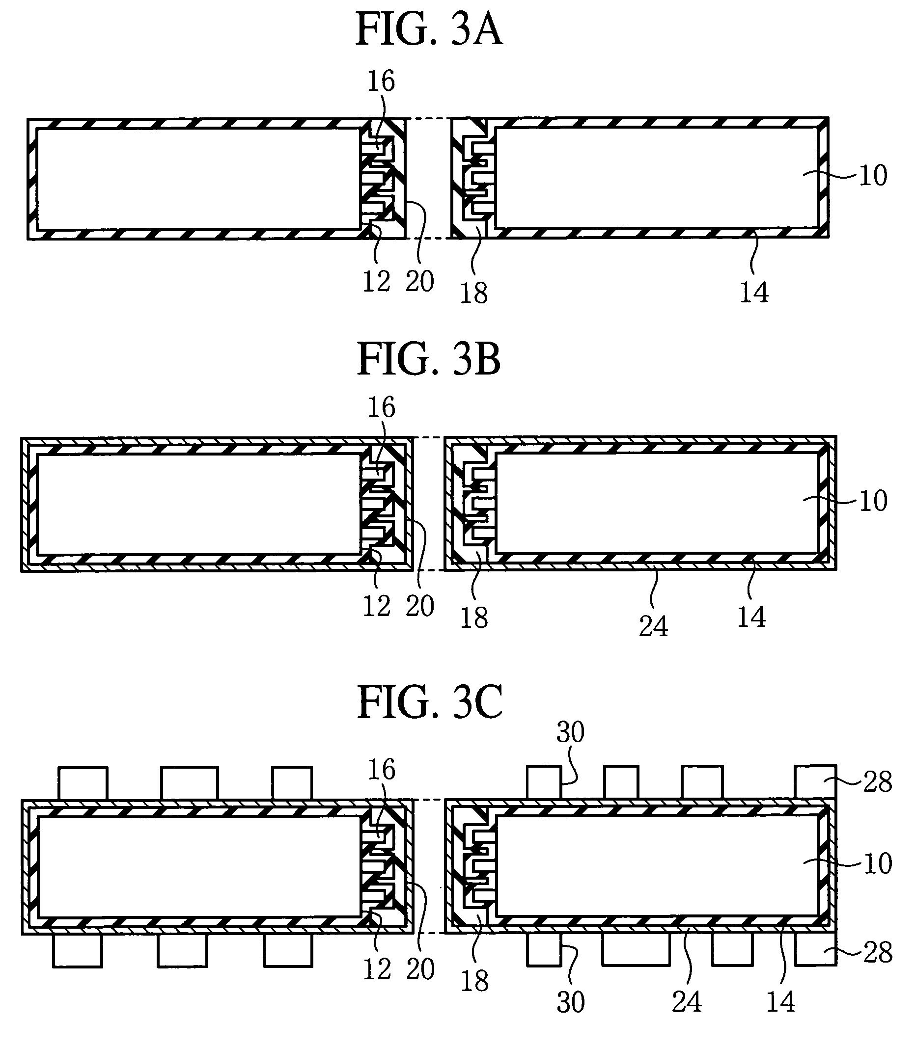
[0029] The wiring board and the method for fabricating the same according to a first embodiment of the present invention will be explained with reference to FIGS. 1, 2A-2C, 3A-3C and 4A-4C. FIG. 1 is a sectional view of the wiring board according to the present embodiment, which illustrates a structure thereof. FIGS. 2A-2C, 3A-3C and 4A-4C are sectional views of the wiring board according to the present embodiment in the steps of the method for fabricating the same, which illustrate the method.

[0030] First, the wiring board according to the present embodiment will be explained with reference to FIG. 1.

[0031] A through-hole 12 is formed throughout a plate-shaped conductive core material 10 from the upper surface thereof to the undersurface thereof. A prescribed number of through-holes 12 corresponding to an wiring layout or others are formed in the conductive core material 10. Specifically, about 1000 through-holes 12, for example, are formed. The diameter of the ...

example 1

[0059] The conductive core material 10 was 5 sheets of the prepreg which was a composite of a 0.2 mm-carbon fiber sheet and a polyimide-group resin composition, which (the prepregs) were laminated by press in a 1.0 mm-thickness. The polyimide resin composition containing the carbon fiber sheet was mixed with an alumina filler by 10 weight % of the whole composition and a silica filler by 10 weight % of the whole composition. The alumina filler had an average particle diameter of below 7 μm including 7 μm and a 7 ppm / K thermal expansion coefficient. The silica filler had an average particle diameter of below 3 μm including 3 μm and a 3 ppm / K thermal expansion coefficient. The conductive core material 10 formed of these materials had, at 25-200° C., a 2 ppm / K average thermal expansion coefficient in the direction of expansion of the surface and a 80 ppm / K average thermal expansion coefficient in the thickness-wise direction. About 1000 through-holes 12 of a 0.5 mm-diameter were formed...

second embodiment

A Second Embodiment

[0066] The wiring board and the method for fabricating the same according to a second embodiment of the present invention will be explained with reference to FIGS. 5A-5B. FIGS. 5A-5B are sectional views of the wiring board according to the present embodiment in the steps of the method for fabricating the same. The same members of the present embodiment as the wiring board and the method for fabricating the same according to the first embodiment are represented by the same reference numbers not to repeat or to simplify their explanation.

[0067] The structure of the wiring board according to the present embodiment is substantially the same as the wiring board according to the first embodiment. The wiring board according to the present embodiment is different from the wiring board according to the first embodiment in that in the former, an insulation layer 14 is formed by electrodeposition. The method for fabricating the wiring board according to the present embodime...


PUM

PropertyMeasurementUnit
Timeaaaaaaaaaa
Electrical conductoraaaaaaaaaa

Abstract

The wiring board comprises a plate-shaped conductive core material 10 with a through-hole 12 formed in, an insulation layer 14 formed on the surface of the conductive core material 10 and on the inside wall of the through-hole 12, a resin 18 buried in the through-hole 12 with the insulation layer 14 formed in, wirings 22a, 22b formed on the upper surface and the undersurface of the conductive core material 10 with the insulation layer 14 formed on, and an wiring 22d formed in the through-hole 20 formed in the resin 18 and electrically connected to the wirings 22a, 22b.

Description

CROSS-REFERENCE TO RELATED APPLICATIONS [0001] This application is based upon and claims priority of Japanese Patent Application No. 2005-033274, filed on Feb. 9, 2005, the contents being incorporated herein by reference. BACKGROUND OF THE INVENTION [0002] The present invention relates to a wiring board and a method for fabricating the same, more specifically, a wiring board including a conductive core material, and a method for fabricating the same. [0003] Recently, electronic apparatuses rapidly have higher performance and are smaller-sized. The semiconductor devices forming the electronic apparatuses, and the wiring boards for the semiconductor devices to be mounted on are required to be accordingly small and thin and to have high performance and high reliability. To meet such requirements, as a semiconductor device mounting technology, bare chip assembly, which mounts semiconductor devices directly on a printed wiring board, is used. [0004] As semiconductor devices have more pin...

Claims


Application Information

Patent Timeline
IPC IPC(8): H05K1/11H05K3/42
CPCH05K1/056H05K3/426H05K3/445H05K2201/0179H05K2201/0195Y10T29/49155H05K2201/09581H05K2203/135Y10T29/49117Y10T29/49165H05K2201/0323
Inventor OKAMOTO, KEISHIROABE, TOMOYUKITANI, MOTOAKIHAYASHI, NOBUYUKI
Owner FUJITSU LTD
Learn More