Membrane-limited selective electroplating of a conductive surface

a selective electroplating and membrane-limited technology, applied in the field of process and apparati, can solve the problem of not being able to disclose a practical method

Inactive Publication Date: 2006-08-10
EI DU PONT DE NEMOURS & CO
View PDF12 Cites 14 Cited by
  • Summary
  • Abstract
  • Description
  • Claims
  • Application Information

AI Technical Summary

Problems solved by technology

Although conventional electroplating technology can provide control over thickness and uniformity of the plated layer, no practical method has been disclosed that selectively deposits a metal layer into the holes and trenches or the recessed areas in the dielectric layer and simultaneously precludes depositing a metallic layer of comparable thickness on top of the plateaus separating the circuit features.

Method used


Image

  • Membrane-limited selective electroplating of a conductive surface
  • Membrane-limited selective electroplating of a conductive surface
  • Membrane-limited selective electroplating of a conductive surface

Examples


Embodiment Construction

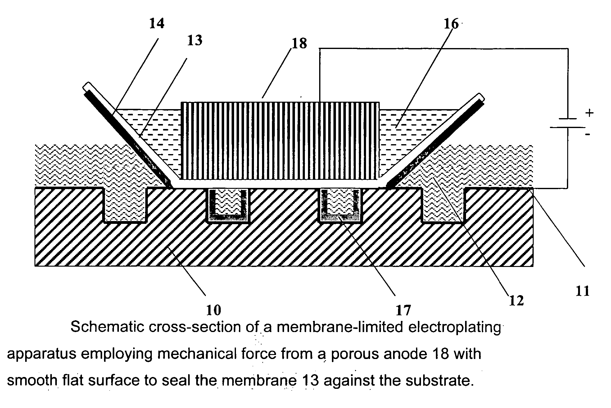
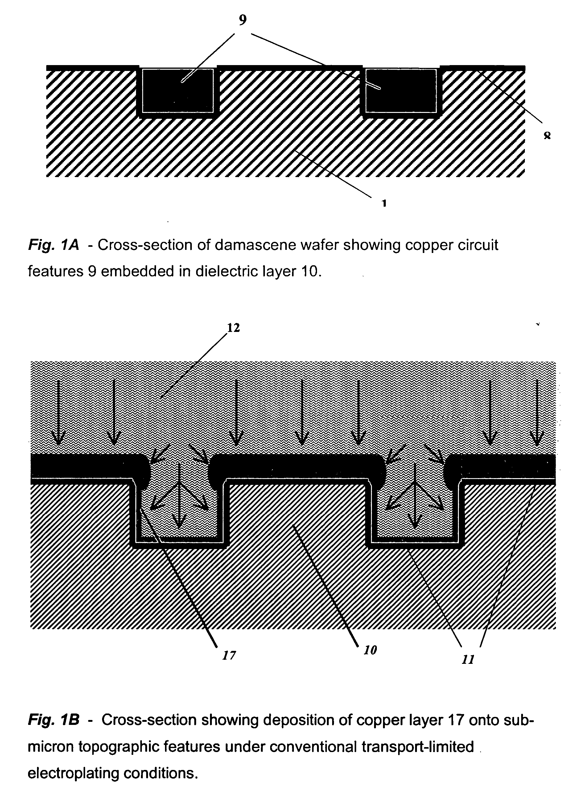
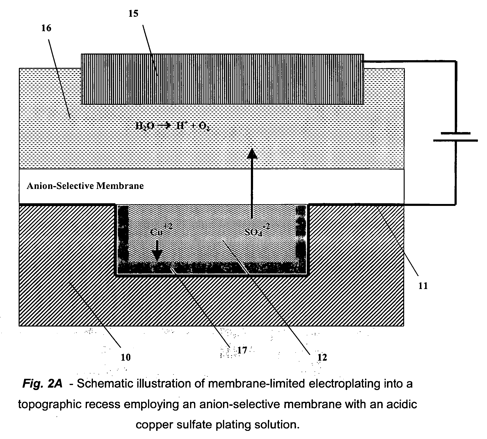
[0025] One embodiment of this invention is an apparatus for electroplating metal onto a conductive surface, the conductive surface comprising plateaus and trenches, the apparatus comprising: [0026] (a) a fluid source providing the conductive surface with an electroplating solution comprising platable metal ions; [0027] (b) a charge-selective ion-conducting membrane comprising a first surface and an opposing second surface, wherein the membrane is substantially impermeable to the platable metal ions in the electroplating solution, and is adapted for the second surface to be placed in close proximity to or in sensible contact with the conductive surface; [0028] (c) an anode in electrical contact with the first surface of the membrane; and [0029] (d) a power source capable applying a voltage between the anode and the conductive surface to generate a flow of electrical current in an amount sufficient to electroplate at least a portion of the metal ions in the electroplating solution ont...


PUM

PropertyMeasurementUnit
pKaaaaaaaaaaa
conductivityaaaaaaaaaa

Abstract

This invention relates to processes and apparati for selectively electroplating a metal layer or layers into recessed topographic features on a conductive surface. The processes and apparati of the invention are useful for fabricating metal circuit patterns, for example for creating copper interconnects between integrated circuit elements embedded in a thin layer of dielectric material on the surface of a semiconductor wafer.

Description

FIELD OF THE INVENTION [0001] This invention relates to processes and apparati for selectively electroplating a metal layer or layers into recessed topographic features on a conductive surface. The processes and apparati of the invention are useful for fabricating metal circuit patterns, for example for creating copper interconnects between integrated circuit elements embedded in a thin layer of dielectric material on the surface of a semiconductor wafer. BACKGROUND [0002] In the damascene process for fabricating integrated circuits, the electrical interconnections are created as patterns of lines and holes etched through a dielectric layer on the surface of the wafer. Such patterns are then filled with metallic copper, and electroplating is commonly used. An ideal deposition process would completely fill the recesses in the dielectric layer with copper to a level that is flush with the surrounding plateau surfaces and not deposit any copper on the plateau surfaces. [0003] Although ...

Claims


Application Information

Patent Timeline
Patent Type & Authority Applications(United States)
IPC IPC(8): C25D7/00C25B9/00
CPCH01L21/2885H01L21/76877H05K3/423H05K2201/09563H05K2203/0557C25D5/02C25D5/34C25D17/008C25D7/123C25D17/001C25D5/04C25D5/18C25D17/002
Inventor MAZUR, STEPHEN
Owner EI DU PONT DE NEMOURS & CO
Why Eureka
Try Eureka