Relaxation of a strained layer using a molten layer

a molten layer and relaxation technology, applied in the field of manufacturing crystalline wafers, can solve the problems of requiring care and implementation, consuming considerable time and expense in the formation of variable compositions in buffer layers,

Active Publication Date: 2006-08-10
S O I TEC SILICON ON INSULATOR THECHNOLOGIES
View PDF18 Cites 33 Cited by
  • Summary
  • Abstract
  • Description
  • Claims
  • Application Information

AI Technical Summary

Benefits of technology

[0015] The invention thus provides a simple manner of relaxing a layer that can have a different lattice parameter than a layer on which it is grown or from which it otherwise depends or is supported.

Problems solved by technology

The formation of the variable composition in the buffer layer takes considerable time and expense and requires care to implement.

Method used


Image

  • Relaxation of a strained layer using a molten layer
  • Relaxation of a strained layer using a molten layer
  • Relaxation of a strained layer using a molten layer

Examples


Embodiment Construction

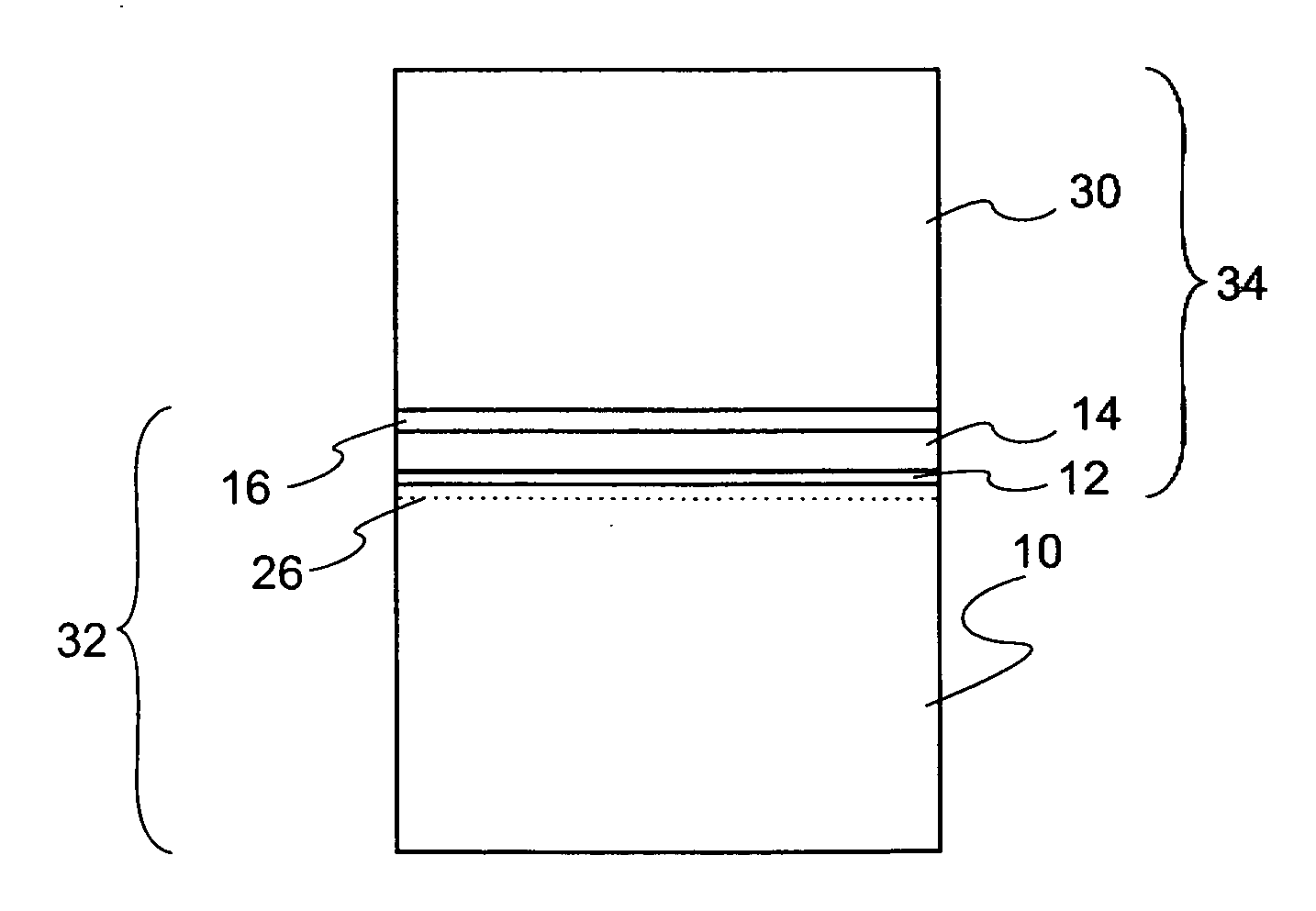
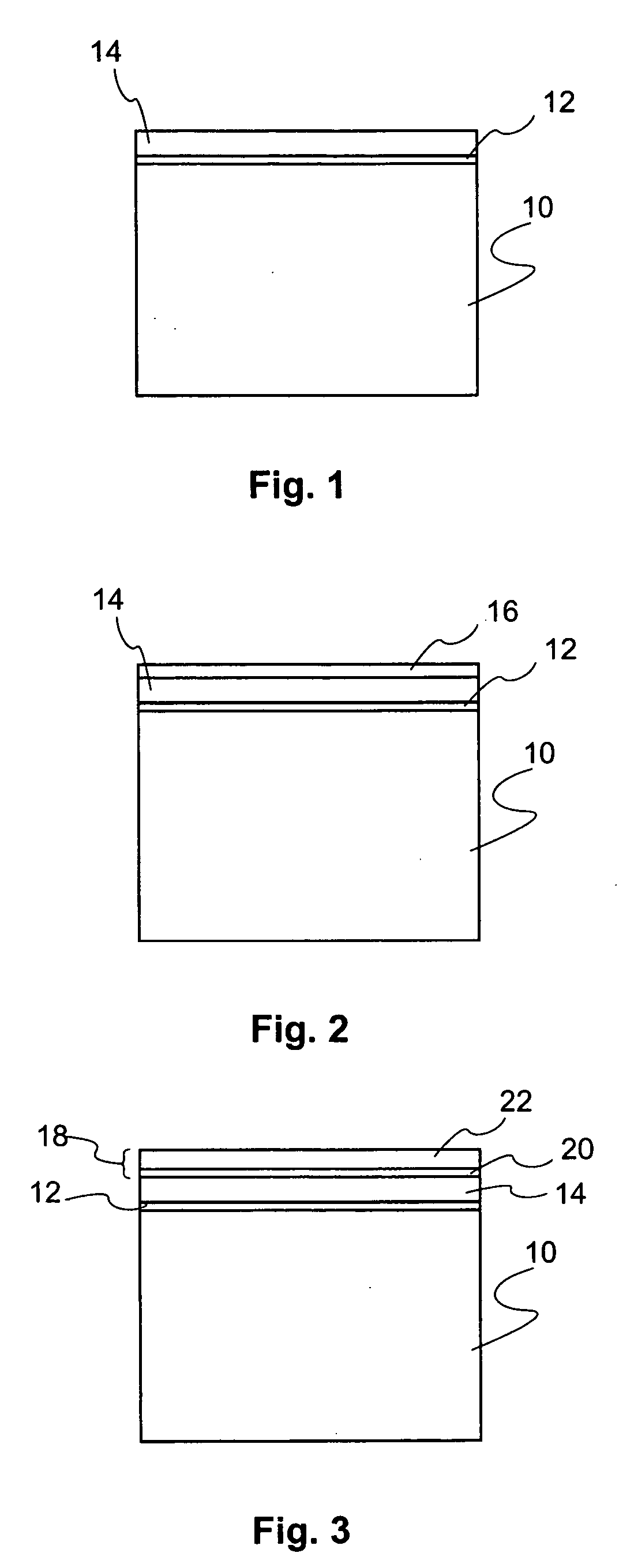
[0022] Referring to FIG. 1, in a preferred method of producing a wafer with a high quality, crystalline relaxed layer, a composite structure is produced. The structure includes support substrate 10, which in the preferred embodiment is made of silicon. The support substrate 10 can alternatively include several layers, preferably with a crystalline layer at its top, such as of a semiconductor material.

[0023] An interface layer 12 is associated with the support substrate 10, and a strained layer 14, which is preferably crystalline, is associated with the interface layer 12. Thus, the interface layer 12 is preferably sandwiched between the support substrate 10 and the strained layer 14.

[0024] Preferably, the nominal lattice parameter of the support substrate 10 and the strained layer 14 are different, such that when associated on the interface layer 12, the strained layer 14 in is a strained state. In the strained state, the crystalline structure of the strained layer 14 is elastical...


PUM


Abstract

A method for making a crystalline wafer, in which an interface layer is associated with a support substrate. A first layer is associated with the interface layer in a strained state. The interface layer is melted sufficiently to substantially uncouple the first layer from the support substrate to relax the first layer from the strained to state to a relaxed state. The interface material is solidified with the first layer in the relaxed state to obtain a first wafer.

Description

FIELD OF THE INVENTION [0001] The present invention relates to the fabrication of crystalline wafers, and more particularly to manufacturing a multicrystalline wafer by melting or heating a layer. BACKGROUND OF THE INVENTION [0002] Certain techniques for manufacturing semiconductor wafers involve producing a layer of a first crystalline material on a substrate of a second crystalline material that has a different nominal lattice parameter. The crystalline structure of the second material is sometimes desired to be relaxed. A known technique provides a buffer layer between the substrate and the produced layer of different nominal lattice parameter. [0003] A typical buffer layer is a transition layer that matches the lattice parameter of the produced layer with that of the substrate. Such a buffer layer may have a composition that gradually varies along its depth by providing the buffer layer with a gradually varying composition. Buffer layers are also known with complex configuration...

Claims


Application Information

Patent Timeline
Patent Type & Authority Applications(United States)
IPC IPC(8): H01L29/04H01L21/46
CPCH01L21/2022H01L21/2026H01L21/02381H01L21/0245H01L21/02532H01L21/02667Y10S438/938
Inventor CELLER, GEORGE K.
Owner S O I TEC SILICON ON INSULATOR THECHNOLOGIES
Why Eureka
Try Eureka