Method and system for programming and driving active matrix light emitting devcie pixel

a technology of active matrix and light-emitting pixel, which is applied in the direction of instruments, static indicating devices, etc., can solve the problems of reducing pixel aperture, reducing yield, and causing image distortion

Active Publication Date: 2006-08-10
IGNIS INNOVATION
View PDF9 Cites 244 Cited by
  • Summary
  • Abstract
  • Description
  • Claims
  • Application Information

AI Technical Summary

Benefits of technology

[0007] It is an object of the invention to provide a method and system that

Problems solved by technology

Since the characteristic parameters of the driving TFT 11, in particular the threshold voltage under bias stress, vary by time, and such changes may differ from pixel to pixel, the induced image distortion may be unacceptably high.
A drawback of U.S. Pat. No. 6,229,508 is that the pixel circuit requires extra tran

Method used


Image

  • Method and system for programming and driving active matrix light emitting devcie pixel
  • Method and system for programming and driving active matrix light emitting devcie pixel
  • Method and system for programming and driving active matrix light emitting devcie pixel

Examples


Embodiment Construction

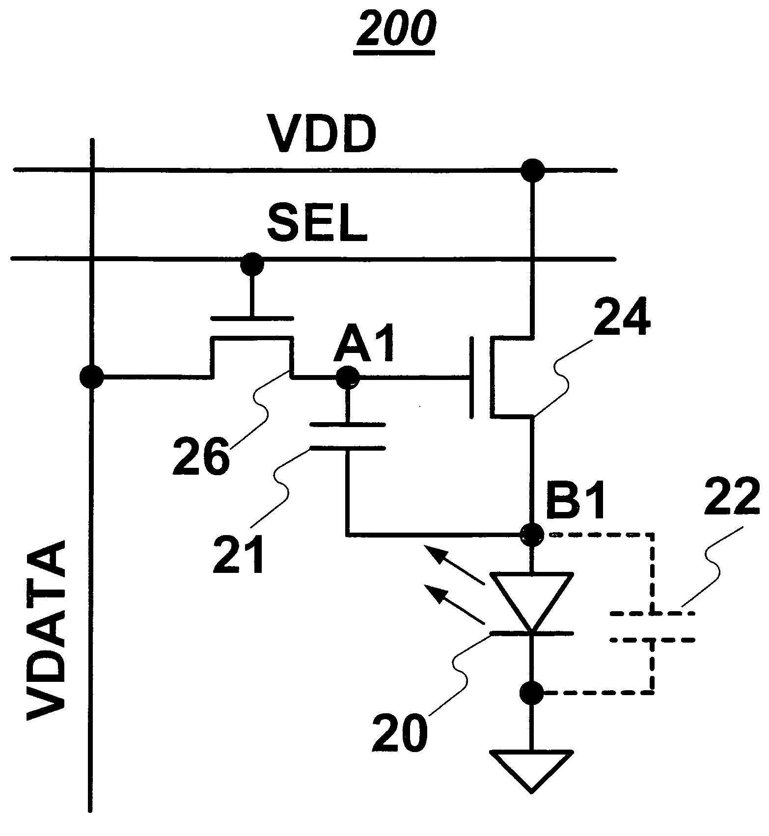
[0038] Embodiments of the present invention are described using a pixel having an organic light emitting diode (OLED) and a driving thin film transistor (TFT). However, the pixel may include any light emitting device other than OLED, and the pixel may include any driving transistor other than TFT. It is noted that in the description, “pixel circuit” and “pixel” may be used interchangeably.

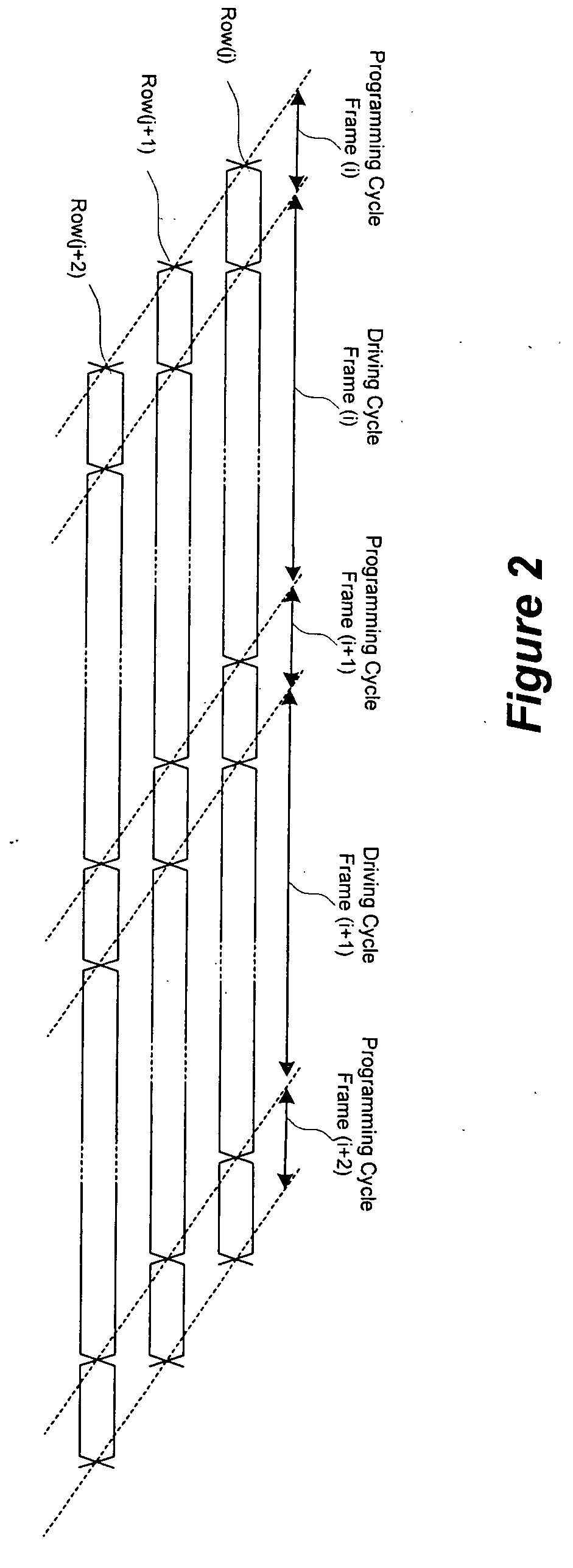
[0039]FIG. 2 is a diagram showing programming and driving cycles in accordance with an embodiment of the present invention. In FIG. 2, each of ROW(j), ROW(j+1), and ROW(j+2) represents a row of the display array where a plurality of pixel circuits are arranged in row and column.

[0040] The programming and driving cycle for a frame occurs after the programming and driving cycle for a next frame. The programming and driving cycles for the frame at a ROW overlaps with the programming and driving cycles for the same frame at a next ROW. As described below, during the programming cycle, the time depend...


PUM


Abstract

Method and system for programming and driving active matrix light emitting device pixel is provided. The pixel is a voltage programmed pixel circuit, and has a light emitting device, a driving transistor and a storage capacitor. The pixel has a programming cycle having a plurality of operating cycles, and a driving cycle. During the programming cycle, the voltage of the connection between the OLED and the driving transistor is controlled so that the desired gate-source voltage of a driving transistor is stored in a storage capacitor.

Description

FIELD OF INVENTION [0001] The present invention relates to a light emitting device displays, and more specifically to a driving technique for the light emitting device displays. BACKGROUND OF THE INVENTION [0002] Recently active-matrix organic light-emitting diode (AMOLED) displays with amorphous silicon (a-Si), poly-silicon, organic, or other driving backplane have become more attractive due to advantages over active matrix liquid crystal displays. An AMOLED display using a-Si backplanes, for example, has the advantages which include low temperature fabrication that broadens the use of different substrates and makes flexible displays feasible, and its low cost fabrication that yields high resolution displays with a wide viewing angle. [0003] The AMOLED display includes an array of rows and columns of pixels, each having an organic light-emitting diode (OLED) and backplane electronics arranged in the array of rows and columns. Since the OLED is a current driven device, the pixel cir...

Claims


Application Information

Patent Timeline
IPC IPC(8): G09G3/30G09G3/3225
CPCG09G3/3233G09G2300/0842G09G2300/0852G09G2310/0262G09G2310/06G09G2310/061G09G2320/043G09G3/3696G09G3/3258G09G2300/0465
Inventor NATHAN, AROKIACHAJI, GHOLAMREZA REZASERVATI, PEYMAN
Owner IGNIS INNOVATION
Why Eureka
Try Eureka