Method of forming a metal interconnection of a semiconductor device, and metal interconnection formed by such method

Active Publication Date: 2006-08-10
SAMSUNG ELECTRONICS CO LTD
View PDF2 Cites 17 Cited by
  • Summary
  • Abstract
  • Description
  • Claims
  • Application Information

AI Technical Summary

Benefits of technology

[0032] According to the method of forming the metal interconnection, the plasma treatment is carried out on the metal layer before the capping insulating layer is formed. Therefore, compressive stress is created in the metal layer and as a result, hillocks are produced at grain boundaries at the surface of the metal layer. In a fine pattern, e.g. a pattern having a CD on the order of micrometers or tens of micromete

Problems solved by technology

However, it is not easy to etch copper, making it very difficult to pattern a copper layer into a desired shape.
The uneven capping insulating layer may be vulnerable to dry etching.
That is, the hillocks impede the ability of inspections associated with each subsequent fabrication process to accurately detect defects.
In this case, a large amount of leakage current occurs and the capacitor exhibits poor electrical properties.
Furthermore, in the conventional method, the grain size of the copper la

Method used


Image

  • Method of forming a metal interconnection of a semiconductor device, and metal interconnection formed by such method
  • Method of forming a metal interconnection of a semiconductor device, and metal interconnection formed by such method
  • Method of forming a metal interconnection of a semiconductor device, and metal interconnection formed by such method

Examples


Embodiment Construction

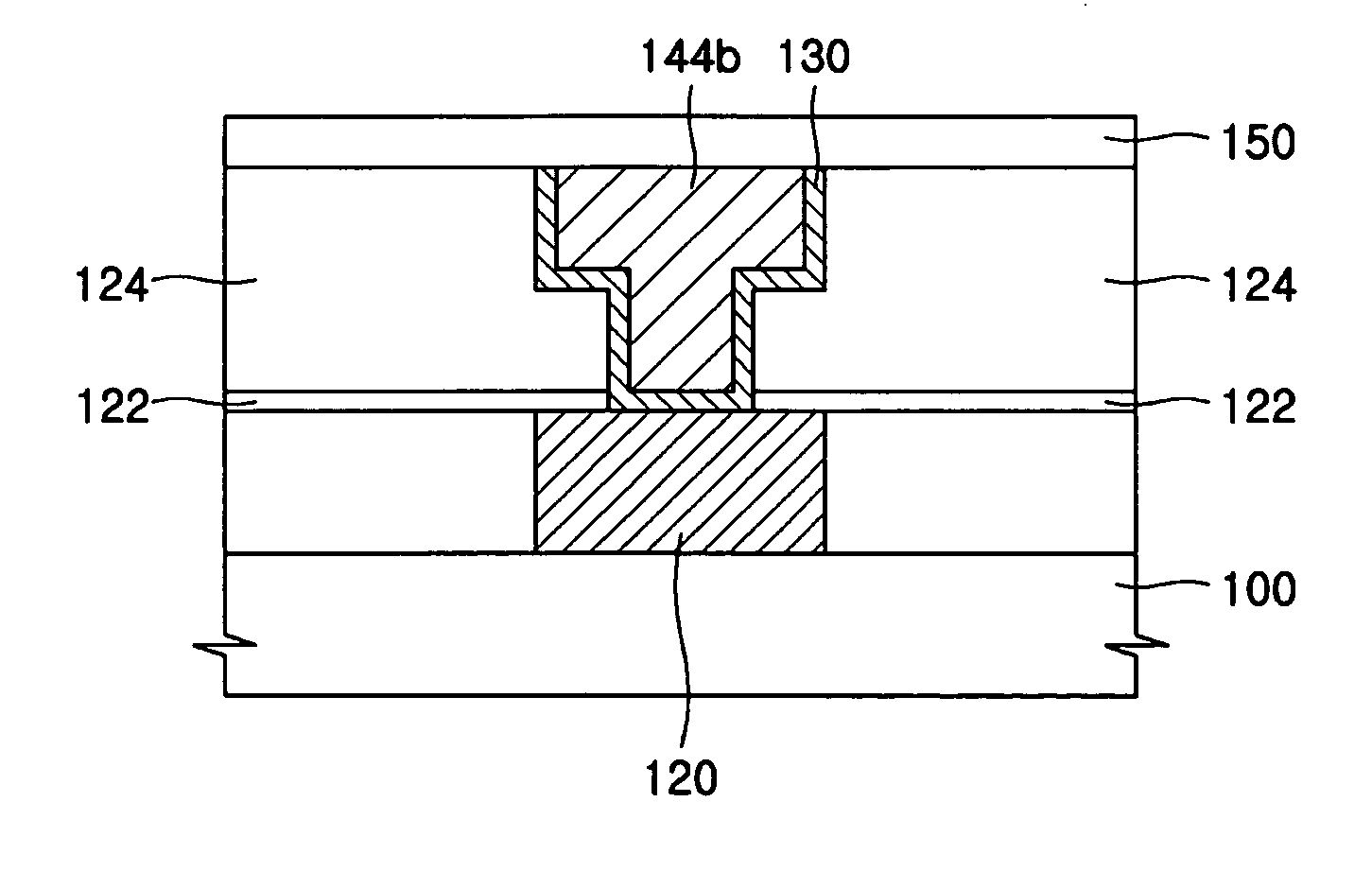
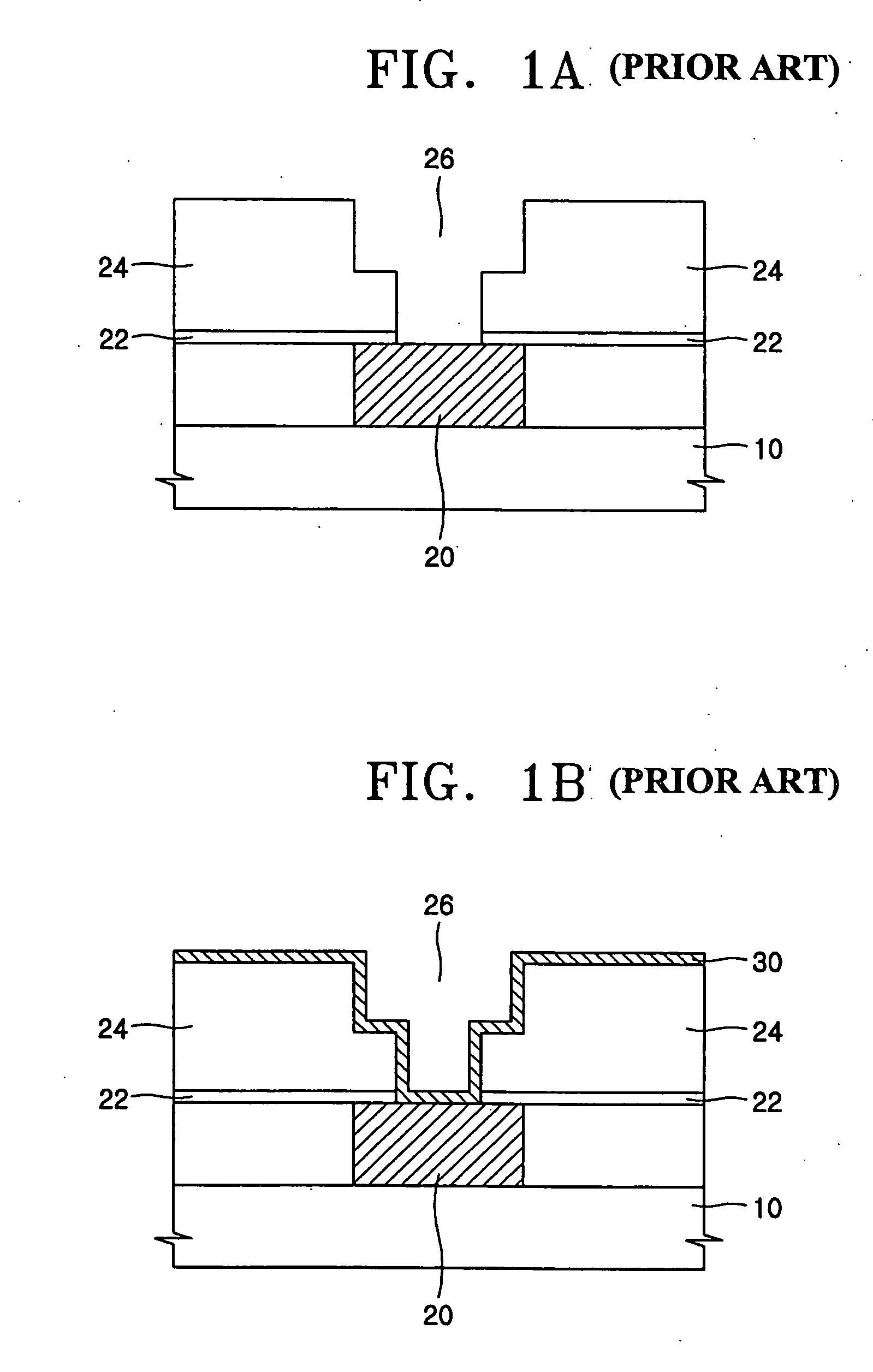
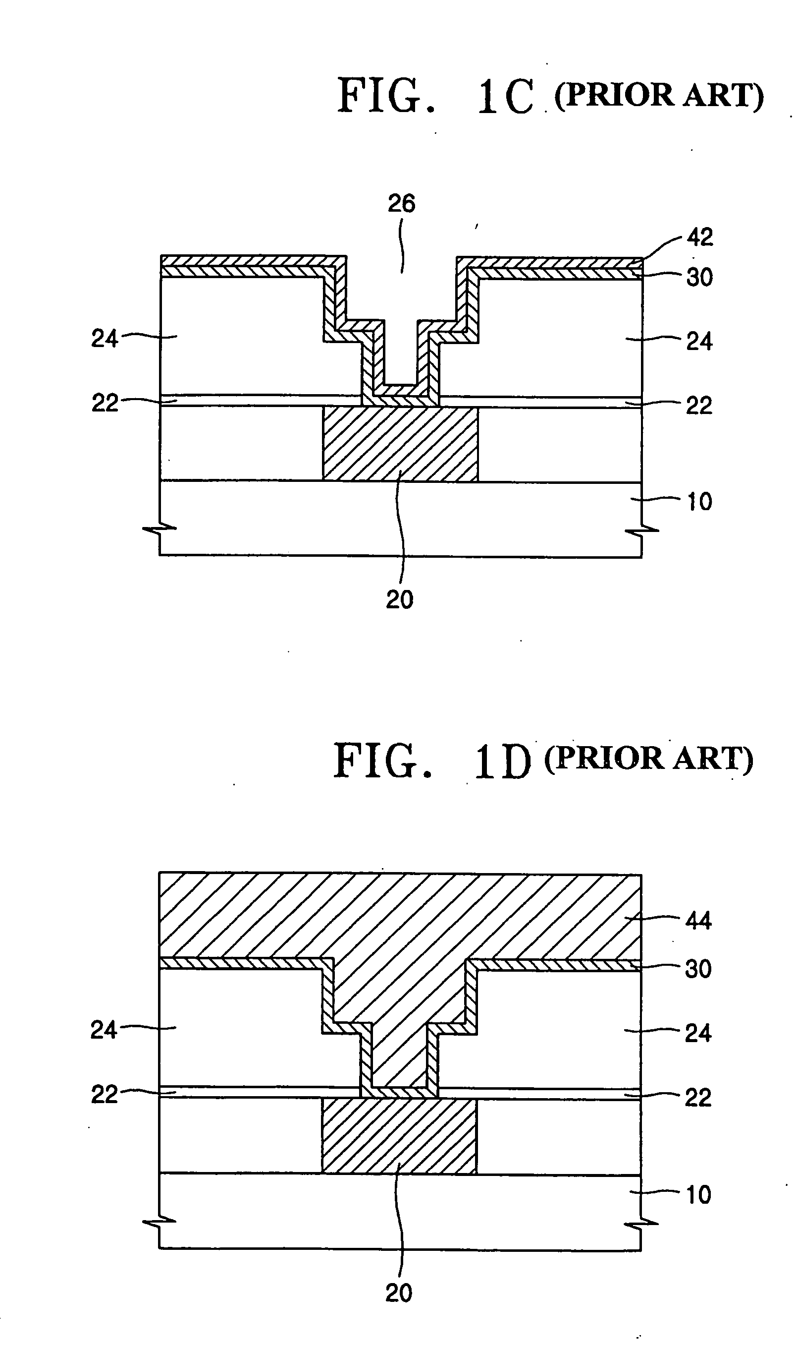
[0043] Referring to FIG. 4A, an interlayer dielectric layer 124 is formed over a semiconductor substrate 100 on which a conductive layer 120, such as a conducive wiring layer, is situated. The interlayer dielectric layer 124 is etched to form an opening 126 therein. For example, the opening 126 may be a dual damascene type of opening that extends through the interlayer dielectric layer 124 and exposes a conductive element of the layer 120. In this case, an etch stop layer 122 may be formed on the conductive layer 120 to prevent the conductive element from being etched when the opening 126 is formed in the interlayer dielectric layer 124. Alternatively, the opening 126 may be in the form of a trench in the interlayer dielectric layer 124, i.e. a recess that does not extend through the interlayer dielectric layer 124.

[0044] Referring to FIG. 4B, a conductive barrier layer 130 is formed on the upper surface of the interlayer dielectric layer 124 and on inner walls of interlayer dielec...


PUM


Abstract

A metal interconnection of a semiconductor device, formed using a damascene process, has large grains and yet a smooth surface. First, a barrier layer and a metal layer are sequentially formed in an opening in an interlayer dielectric layer. A CMP process is carried out on the metal layer to form a metal interconnection remaining within the opening. Then, the metal interconnection is treated with plasma. The plasma treatment creates compressive stress in the metal interconnection, which stress produces hillocks at the surface of the metal interconnection. In addition, the plasma treatment process causes grains of the metal to grow, especially when the design rule is small, to thereby decrease the resistivity of the metal interconnection. The hillocks are then removed by a CMP process aimed at polishing the portion of the barrier layer that extends over the upper surface of the interlayer dielectric layer. Finally, a capping insulating layer is formed. The intentional forming of hillocks by the plasma treatment process at weak portions of the metal interconnection and the subsequent removal of the hillocks greatly reduces the possibility of any additional hillocks being produced at the surface of the metal interconnection, especially when the capping layer is formed.

Description

BACKGROUND OF THE INVENTION [0001] 1. Field of the Invention [0002] The present invention relates to a method of manufacturing a metal interconnection of a semiconductor device. More particularly, the present invention relates to a damascene process used to form metal interconnections of a semiconductor device. [0003] 2. Description of the Related Art [0004] Copper (Cu) is widely used for forming metal interconnections of highly integrated semiconductor devices. Although the resistivity of aluminum (Al) is about 2.67 μΩ·cm, the resistivity of copper is 1.69 μΩ·cm. Therefore, the lower resistivity of Cu allows Cu patterns to transmit signals at higher rates than similar Al patterns. In addition, Cu patterns have a great resistance to electromigration (EM), which enhances the reliability of semiconductor devices. Furthermore, Cu is a useful material for forming interconnections because the power consumption of Cu is relatively small and Cu is less expensive as a raw material than Al. ...

Claims


Application Information

Patent Timeline
IPC IPC(8): B32B3/04
CPCH01L21/7684Y10T428/24207H01L21/76883H01L21/76877
Inventor LEE, SUN-JUNGLEE, SOO-GEUNSHIN, HONG-JAEKIM, ANDREW-TAECHOI, SEUNG-MANSUH, BONG-SEOK
Owner SAMSUNG ELECTRONICS CO LTD
Why Eureka
Try Eureka