Use of germanium dioxide and/or alloys of GeO2 with silicon dioxide for semiconductor dielectric applications

a technology of germanium dioxide and/or alloys, applied in the direction of semiconductor/solid-state device manufacturing, basic electric elements, electric apparatus, etc., can solve the problems of difficult to completely fill the gap of semiconductor manufacturers, adversely affecting device operation, and difficult to fill high-aspect-ratio gaps, etc., to achieve the effect of increasing the bias power

Inactive Publication Date: 2006-08-10
APPLIED MATERIALS INC
View PDF6 Cites 14 Cited by
  • Summary
  • Abstract
  • Description
  • Claims
  • Application Information

AI Technical Summary

Benefits of technology

[0011] Still another embodiment of the method of the invention comprises depositing a first portion of the dielectric film during a first deposition stage by flowing a process gas comprising a germanium source, a silicon source and an oxidizing agent into the substrate processing chamber; forming a high density plasma that has simultaneous deposition and sputtering components from the process gas; and maintaining a pressure within the substrate processing chamber of less than 100 mTorr; and depositing a second portion of the dielectric film during a second deposition stage, after the first stage, by increasing bias power applied to the substrate processing chamber to heat the dielectric film close to or above its glass transition temperature while maintaining the flow of the process gas into the substrate processing chamber.

Problems solved by technology

Gaps having a combination of high aspect ratio and a small width present a particular challenge for semiconductor manufacturers to fill completely.
In short, the challenge usually is to prevent the deposited film from growing in a manner that closes off the gap before it is filled.
Failure to fill the gap completely results in the formation of voids in the deposited layer, which may adversely affect device operation.
High-aspect-ratio gaps are difficult to fill using conventional CVD methods, causing some integrated-circuit manufacturers to turn to the use high-density-plasma CVD (“HDP-CVD”) techniques.
Semiconductor manufacturers have discovered, however, that there is a practical limit to the aspect ratio of gaps that HDP-CVD deposition techniques are able to fill.

Method used


Image

  • Use of germanium dioxide and/or alloys of GeO2 with silicon dioxide for semiconductor dielectric applications
  • Use of germanium dioxide and/or alloys of GeO2 with silicon dioxide for semiconductor dielectric applications
  • Use of germanium dioxide and/or alloys of GeO2 with silicon dioxide for semiconductor dielectric applications

Examples


Embodiment Construction

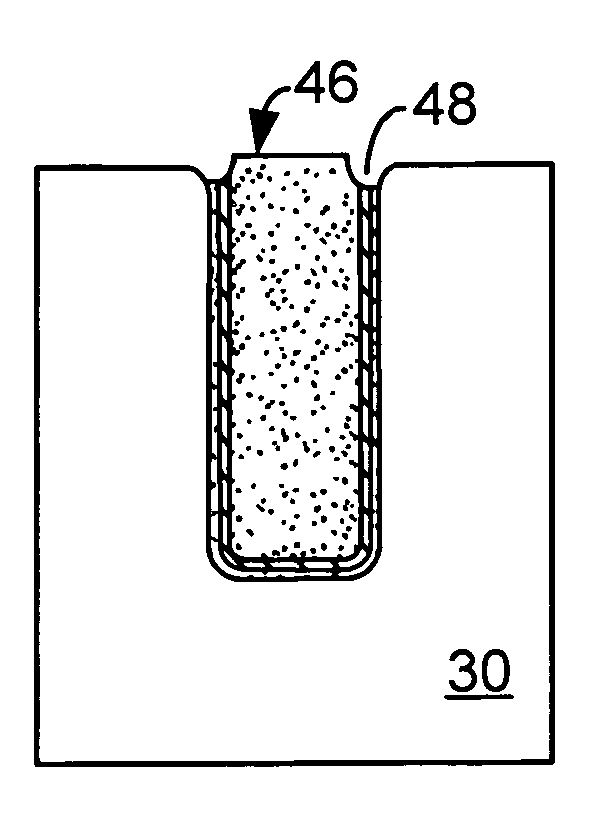
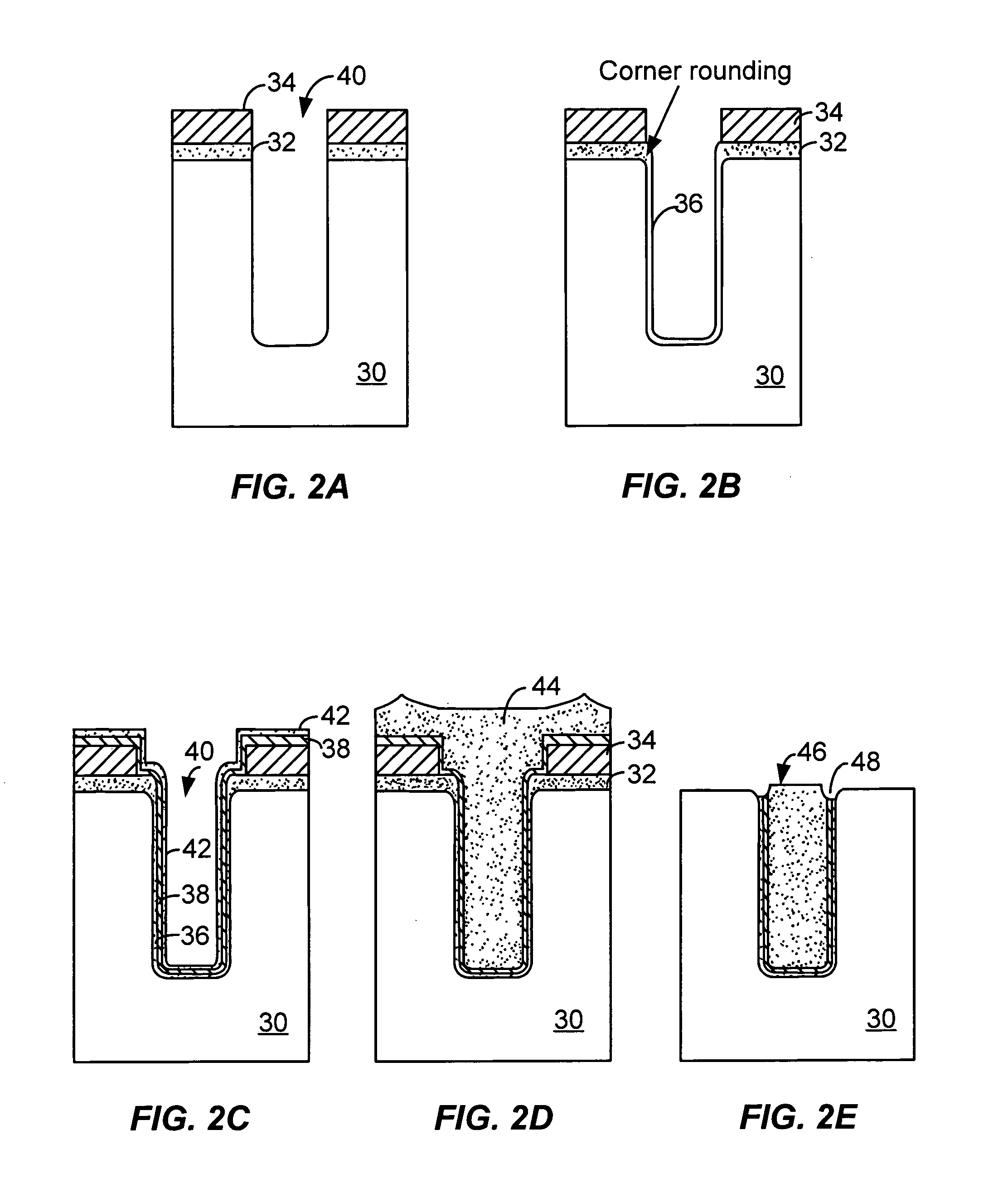
[0021] Embodiments of the invention fill trenches and / or gaps between adjacent raised features of integrated circuits by depositing an insulating material that contains silicon, germanium and oxygen into the trenches and / or gaps. The ratio of silicon to germanium in the film may vary depending on the film's application as discussed in detail below. Embodiments of the invention can be used to fill STI trenches, gaps formed between adjacent vertical transistors and other gaps or trenches formed between raised structures formed on a substrate when the substrate can be heated to a temperature close to or above the reflow temperature of the deposited film. Embodiments of the invention permit the dielectric material to be deposited with substantially 100% gapfill for integrated circuits having minimum feature sizes of 0.10 μm or less that include very aggressive gapfill structures having aspect ratios greater than 6:1.

[0022] As used herein, references to an HDP-CVD process are intended t...


PUM

PropertyMeasurementUnit
pressureaaaaaaaaaa
feature sizesaaaaaaaaaa
pressureaaaaaaaaaa

Abstract

A method is disclosed for depositing a dielectric film on a substrate having a plurality of gaps formed between adjacent raised surfaces disposed in a high density plasma substrate processing chamber substrate. In one embodiment the method comprises flowing a process gas comprising a germanium source, a silicon source and an oxidizing agent into the substrate processing chamber; forming a high density plasma that has simultaneous deposition and sputtering components from the process gas to deposit a dielectric film comprising silicon, germanium and oxygen; and during the step of forming a high density plasma, maintaining a pressure within the substrate processing chamber of less than 100 mTorr while allowing the dielectric film to be heated above its glass transition temperature.

Description

BACKGROUND OF THE INVENTION [0001] One common step that may be performed frequently during fabrication of modern semiconductor devices is the formation of a thin film on a semiconductor substrate by chemical reaction of gases. Such deposition processes are referred to generally as chemical vapor deposition (“CVD”) and include both thermal CVD processes and plasma-enhanced CVD (“PECVD”) process. In conventional thermal CVD processes, reactive gases are supplied to the substrate surface, where heat-induced chemical reactions take place to form the desired film. In a conventional plasma process, a controlled plasma is formed to decompose and / or energize reactive species to produce the desired film. [0002] Any of these CVD techniques may be used to deposit conductive or insulative films during the fabrication of integrated circuits. One important physical property of CVD insulative films includes the film's ability to fill gaps completely between adjacent structures without leaving void...

Claims


Application Information

Patent Timeline
Patent Type & Authority Applications(United States)
IPC IPC(8): H01L21/4763H01L21/31
CPCH01L21/02126H01L21/02274H01L21/0234H01L21/31604H01L21/31612H01L21/76224H01L21/76837
Inventor KRISHNARAJ, PADMANABHANCOX, MICHAEL S.GEOFFRION, BRUNONEMANI, SRINIVAS D.
Owner APPLIED MATERIALS INC
Why Eureka
Try Eureka