Synchronous data transfer circuit, computer system and memory system

a data transfer circuit and computer system technology, applied in the direction of generating/distributing signals, pulse techniques, instruments, etc., can solve the problems of difficult to dispose of a plurality of modules (chips) with the same distance from other modules (chips), the range of the above dispersion becomes difficult to ignore, and the method is not applicable without modification, so as to reduce the number of delay elements and reduce the mounting area of the delay circuit

Active Publication Date: 2006-08-17
FUJITSU LTD
View PDF9 Cites 8 Cited by
  • Summary
  • Abstract
  • Description
  • Claims
  • Application Information

AI Technical Summary

Benefits of technology

[0024] Accordingly, it is an object of the present invention to provide a synchronous data transfer circuit, a computer system and a memory system, reducing the number of delay elements required for a plurality of read control circuit, thereby reducing the mounting area of the delay circuits in a chip.

Problems solved by technology

In such an apparatus, as a matter of mounting, it is difficult to dispose a plurality of modules (chips) with the same distance from other modules (chips).
With the improvement of data processing speed in recent years, the range of the above dispersion becomes hard to ignore.
However, since fine tuning is further required in an IC chip for transfer to another IC chip being connected, the above method is not applicable without modification.
Meanwhile, as shown in FIG. 8, when the chip 200 of data request target outputs a 64-bit parallel signal, dispersion in each signal is substantially large, which makes it difficult to cope with the dispersion by one data strobe signal DQ [N:0].
This necessitates that a large number of delay elements have been required in each delay circuit.
This necessitates a large mounting area on the circuit (chip), which impedes miniaturization and low cost.
Also since the power consumption becomes large, it has been difficult to produce the chip with low power consumption.
In addition, the delay element using transistors has a large dispersion of the delay amount, producing a deduced delay accuracy, and impeding high-speed synchronous transfer.

Method used


Image

  • Synchronous data transfer circuit, computer system and memory system
  • Synchronous data transfer circuit, computer system and memory system
  • Synchronous data transfer circuit, computer system and memory system

Examples


Embodiment Construction

[0050] The preferred embodiment of the present invention is described herein after referring to the charts and drawings, in order of a computer system, a synchronous data transfer circuit, and other embodiments.

Computer System

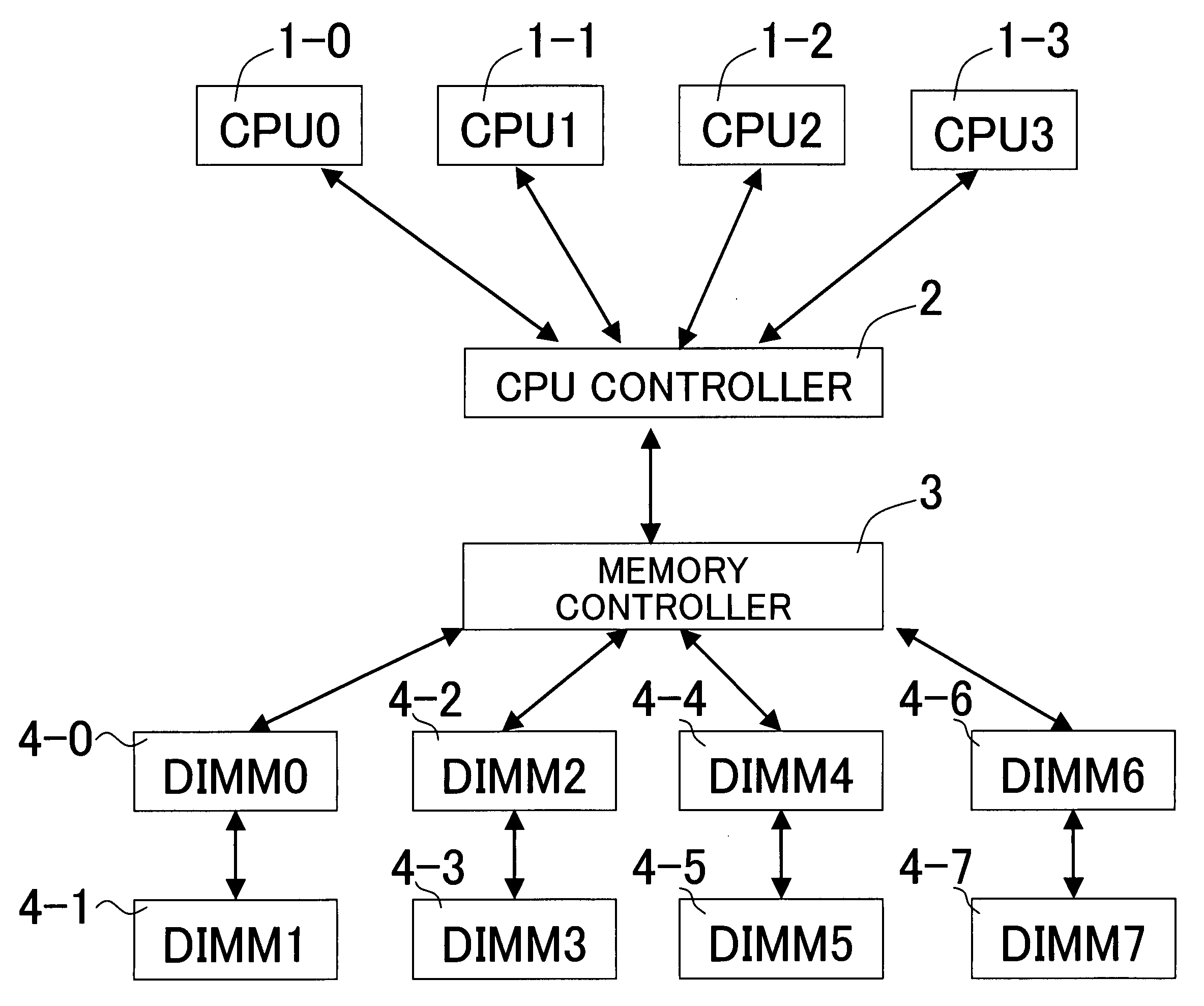
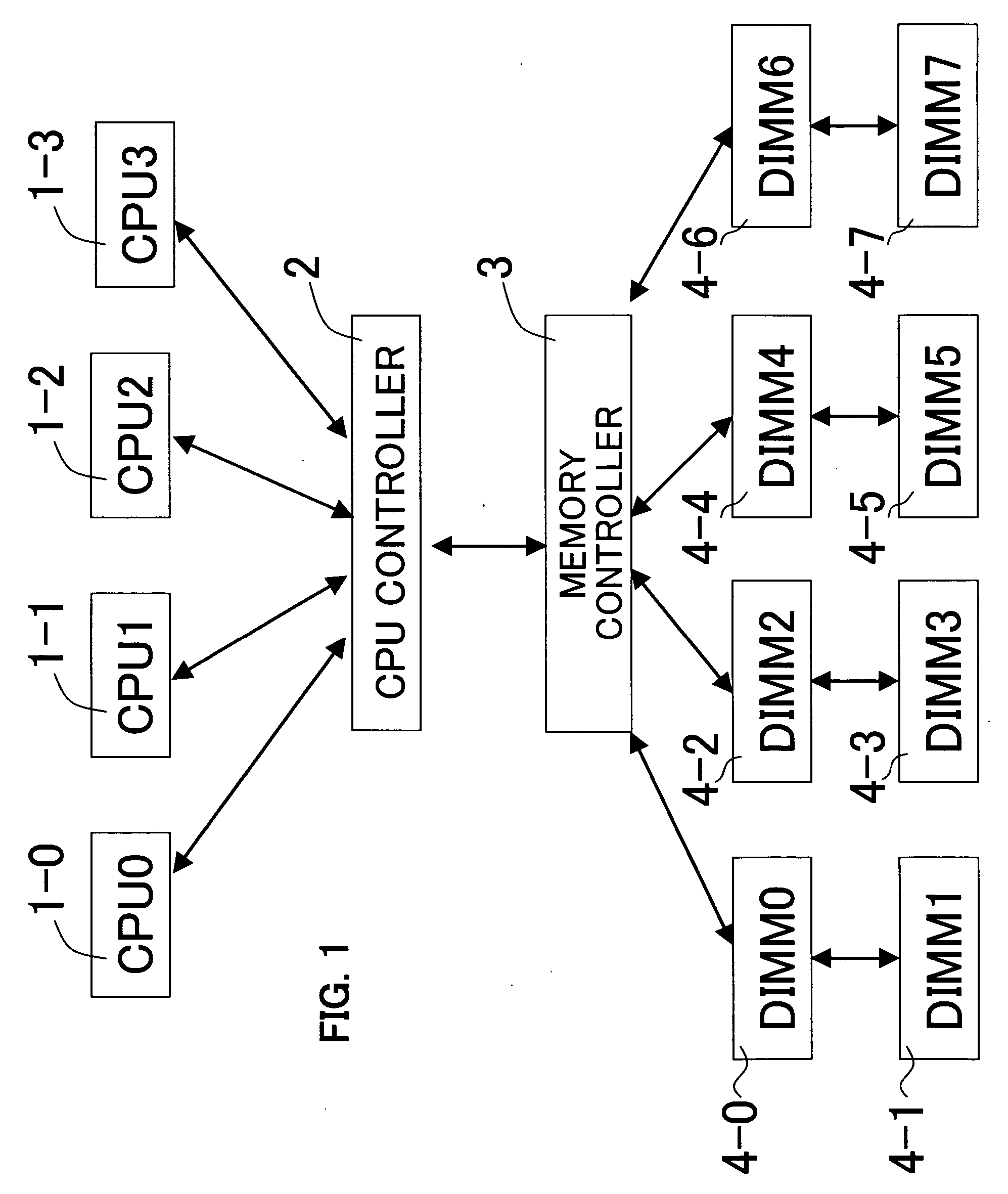
[0051]FIG. 1 shows a configuration diagram of a computer system according to one embodiment of the present invention. FIG. 2 shows a mounting diagram of the memory system shown in FIG. 1. In the above FIG. 1, a configuration of a computer board provided in a server is shown.

[0052] As shown in FIG. 1, on the computer board, four CPUs (central processor units) 1-0, 1-1, 1-2 and 1-3, a CPU control circuit 2, a memory control circuit 3, and eight DIMMs (dual in-line memory modules) 4-0 to 4-7 which constitute a main memory module are mounted. DIMMs 4-0 to 4-7 are modules having DRAM (dynamic random access memory) chips mounted thereon, having a data bus width of 64 bits.

[0053] Eight DIMMs 4-0 to 4-7 are connected to the memory control circuit 3 at the unit of ...


PUM


Abstract

A circuit synchronizes parallel data of different timing for transfer. The synchronous data transfer circuit includes a plurality of first flip-flop circuits in which the parallel data are set by a data strobe signal, a plurality of delay circuits, and a plurality of second flip-flop circuits. By configuring the second flip-flop circuits to share generation of a delay amount, the second flip-flop circuits are utilized for data synchronization by the synchronous data transfer circuit. Thus, it becomes possible to configure the delay circuits with a remarkably reduced amount of delay elements.

Description

CROSS-REFERENCE TO RELATED APPLICATIONS [0001] This application is based upon and claims the benefit of priority from the prior Japanese Patent Application No. 2005-023592, filed on Jan. 31, 2005, the entire contents of which are incorporated herein by reference. BACKGROUND OF THE INVENTION [0002] 1. Field of the Invention [0003] The present invention relates to a synchronous data transfer circuit, a computer system and a memory system, for reading and transferring data from a circuit chip disposed on a substrate, and more particularly a synchronous data transfer circuit, a computer system and a memory system for transferring data at the same timing even a delay amount of the data from a circuit chip differs. [0004] 2. Description of the Related Art [0005] With the development of the semiconductor technology and a chip mounting technique, there has been provided an apparatus on which a plurality of CPUs and a large capacity main memory device are mounted on a single substrate. For e...

Claims


Application Information

Patent Timeline
Patent Type & Authority Applications(United States)
IPC IPC(8): G06F11/00
CPCG06F13/1689G11C7/1051G11C7/106Y02B60/1228G11C7/22G11C7/222H03K5/135G11C7/1066Y02D10/00G06F12/00G11C7/00G11C11/407
Inventor SAKAMAKI, HIDEYUKI
Owner FUJITSU LTD
Why Eureka
Try Eureka