Method and program for generating layout data of a semiconductor integrated circuit and method for manufacturing a semiconductor integrated circuit with optical proximity correction

Inactive Publication Date: 2006-08-17
KK TOSHIBA
View PDF3 Cites 20 Cited by
  • Summary
  • Abstract
  • Description
  • Claims
  • Application Information

AI Technical Summary

Problems solved by technology

In such cases, during a photolithography process or an etching process, the planar shape of an element pattern in the periphery of an element to be formed adversely affects the planar shape of the element pattern to be formed.
As a result, i

Method used


Image

  • Method and program for generating layout data of a semiconductor integrated circuit and method for manufacturing a semiconductor integrated circuit with optical proximity correction
  • Method and program for generating layout data of a semiconductor integrated circuit and method for manufacturing a semiconductor integrated circuit with optical proximity correction
  • Method and program for generating layout data of a semiconductor integrated circuit and method for manufacturing a semiconductor integrated circuit with optical proximity correction

Examples


modified example

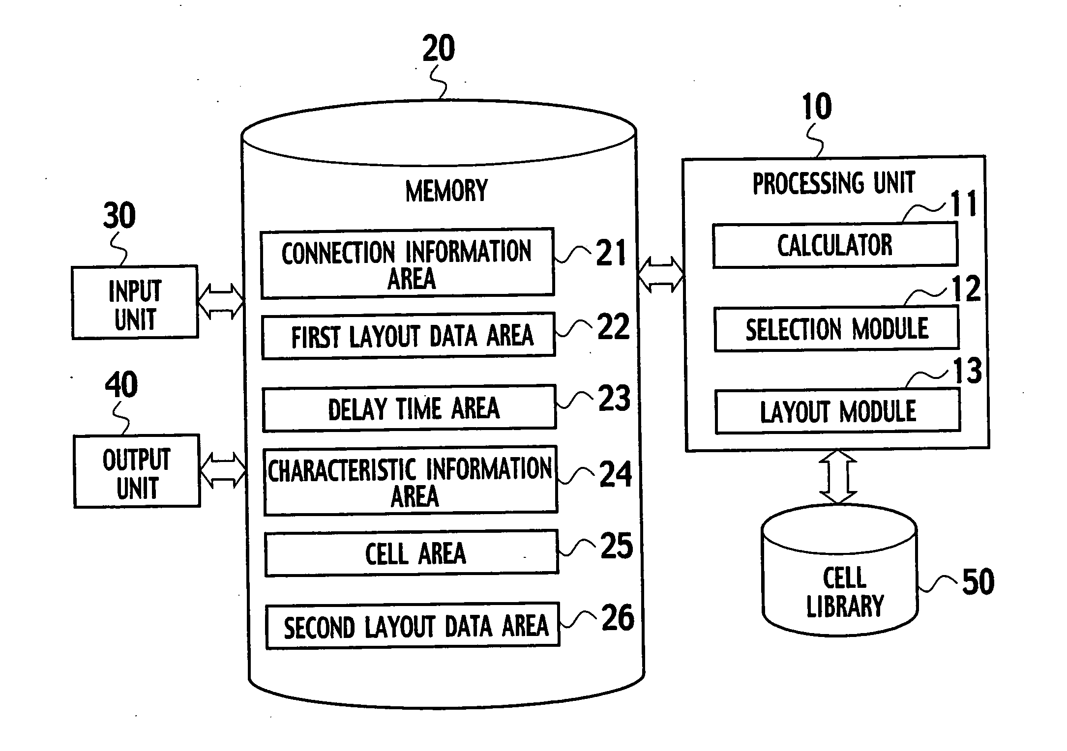
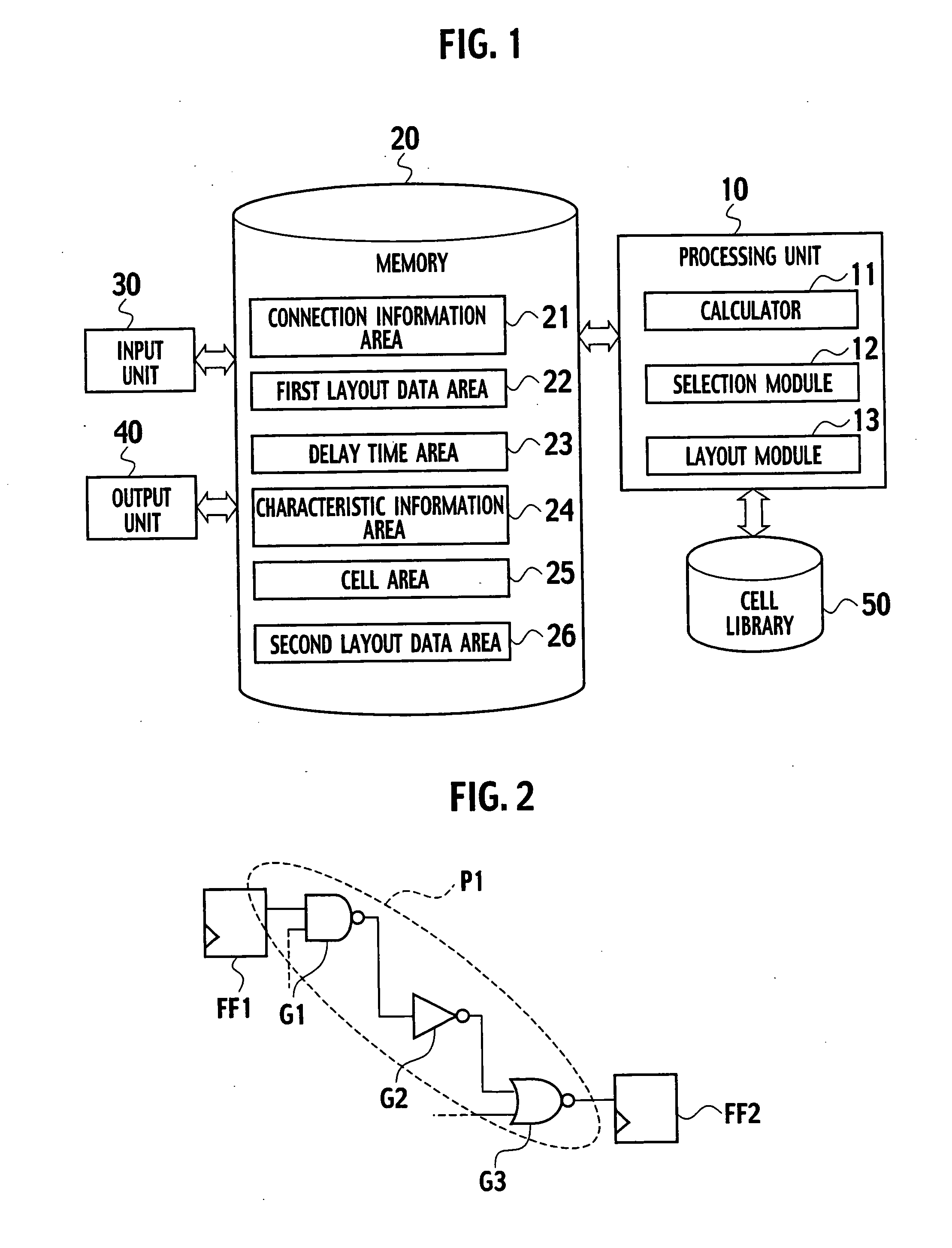
[0101] An example where cell patterns corresponding to cells included along a signal propagating path that is not a critical path are replaced by cell patterns generated based on relaxed dimensional tolerance conditions has been described above. However, the delay time, calculated based on the layout information of the circuit elements stored in the first layout data area 22 of FIG. 1 before the cell patterns are replaced, may fail to satisfy the allowable delay time. For example, when the cell patterns included in the cell pattern group C1 are selected, it is assumed that there be a cell with a delay time being highly sensitive to non-uniform processing among the 2-input NAND cell G1, the inverter cell G2, and the 2-input NOR cell G3 included along the path P1 shown in FIG. 2. As a result, the calculated delay time td1 for the path P1 is also highly sensitive to non-uniform processing. In other words, the calculated delay time td1 for the path P1 may exceed an allowable delay time ...


PUM


Abstract

A method for generating layout data of a semiconductor integrated circuit includes applying optical proximity correction conditions to cells so as to generate cell patterns, selecting cell patterns to correspond cells, based on layout information of cells along a specified signal propagating path; calculating delay times for the signal propagating path for combinations of cell patterns; selecting a combination of cell patterns, based on lengths of the calculated delay times and the allowable delay time; and generating layout data of the signal propagating path using the selected combination.

Description

CROSS REFERENCE TO RELATED APPLICATIONS AND INCORPORATION BY REFERENCE [0001] This application is based upon and claims the benefit of priority from prior Japanese Patent Application P2005-032243 filed on Feb. 8, 2005; the entire contents of which are incorporated by reference herein. BACKGROUND OF THE INVENTION [0002] 1. Field of the Invention [0003] The present invention relates to a layout method of a semiconductor integrated circuit, particularly for an automatic layouting method and a program for generating layout data of a semiconductor integrated circuit, and a method for manufacturing a semiconductor integrated circuit with optical proximity correction. [0004] 2. Description of the Related Art [0005] Along with the miniaturization of elements such as transistors or interconnects used in semiconductor integrated circuits, the size of element has become smaller than light source wavelengths used for an aligner. In such cases, during a photolithography process or an etching pro...

Claims


Application Information

Patent Timeline
IPC IPC(8): G06F17/50G03F1/36G03F1/68G03F1/70H01L21/027
CPCG03F1/144G03F1/36G06F17/5068G06F30/39
Inventor MINAMI, FUMIHIROKOTANI, TOSHIYA
Owner KK TOSHIBA
Why Eureka
Try Eureka