Display device and manufacturing method of the same

a technology of display device and manufacturing method, which is applied in the direction of semiconductor devices, instruments, electrical devices, etc., can solve the problems of reliability, easy deterioration of light-emitting elements using organic materials, and easy deterioration of light-emitting elements, etc., and achieves a large increase in processing steps and high moisture permeability.

Active Publication Date: 2006-08-24
SEMICON ENERGY LAB CO LTD
View PDF27 Cites 65 Cited by
  • Summary
  • Abstract
  • Description
  • Claims
  • Application Information

AI Technical Summary

Benefits of technology

[0020] In accordance with a method for manufacturing a display device of the present invention, a light-emitting device in which unevenness generated under a light-emitting element does not impart an adverse effect on the light-emitting element can be manufactured. Further, a light-emitting device in which penetration of water into the inside of the light-emitting device through a film having high moisture permeability can be suppressed without increasing processing steps considerably can be manufactured. Furthermore, a light-emitting device satisfying the above two simultaneously can be manufactured.

Problems solved by technology

However, one background of not reaching practical use yet while having such big advantages is a problem of reliability.
The light-emitting element using an organic-based material often deteriorates due to moisture (water) and has a disadvantage of being hard to obtain long-term reliability.
It is conceivable that this causes a dark spot (black spot) and shrinkage (decrease in luminance from an edge portion of a display device) in a display device using the light-emitting element.
However, these countermeasures are not enough to obtain sufficient reliability of the light-emitting element; thus, it is desired to further improve the reliability.
In addition, since a thin film light-emitting element is formed by laminating extremely thin films, the film and wiring covering an uneven portion is cut due to unevenness under the light-emitting element, which causes a defect.

Method used


Image

  • Display device and manufacturing method of the same
  • Display device and manufacturing method of the same
  • Display device and manufacturing method of the same

Examples


embodiment mode 1

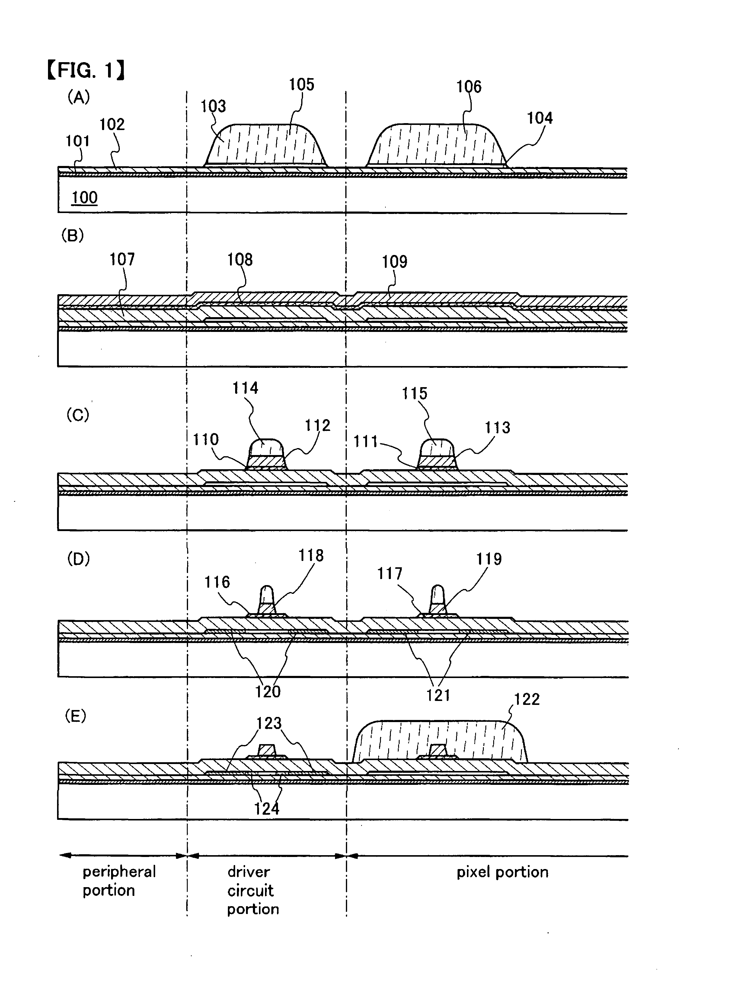
[0048] A method for manufacturing a display device of the present invention will be described with reference to FIGS. 1 to 4.

[0049] First, a first base insulating film 101 and a second base insulating film 102 are formed over a substrate 100, and a semiconductor layer is then formed over the second base insulating film 102. The semiconductor layer is etched with the use of masks 105 and 106 of photoresist or the like in order to form island-shaped semiconductor layers 103 and 104 (FIG. 1A).

[0050] Glass, quartz, plastic (such as polyimide, acrylic, polyethylene terephthalate, polycarbonate, polyacrylate, or polyethersulfone), or the like can be used as a material of the substrate 100. The substrate thereof may be used after being polished by CMP or the like, if necessary. In this Embodiment Mode, a glass substrate is used.

[0051] The first base insulating film 101 and the second base insulating film 102 are formed in order to prevent an element imparting an adverse effect on charac...

embodiment mode 2

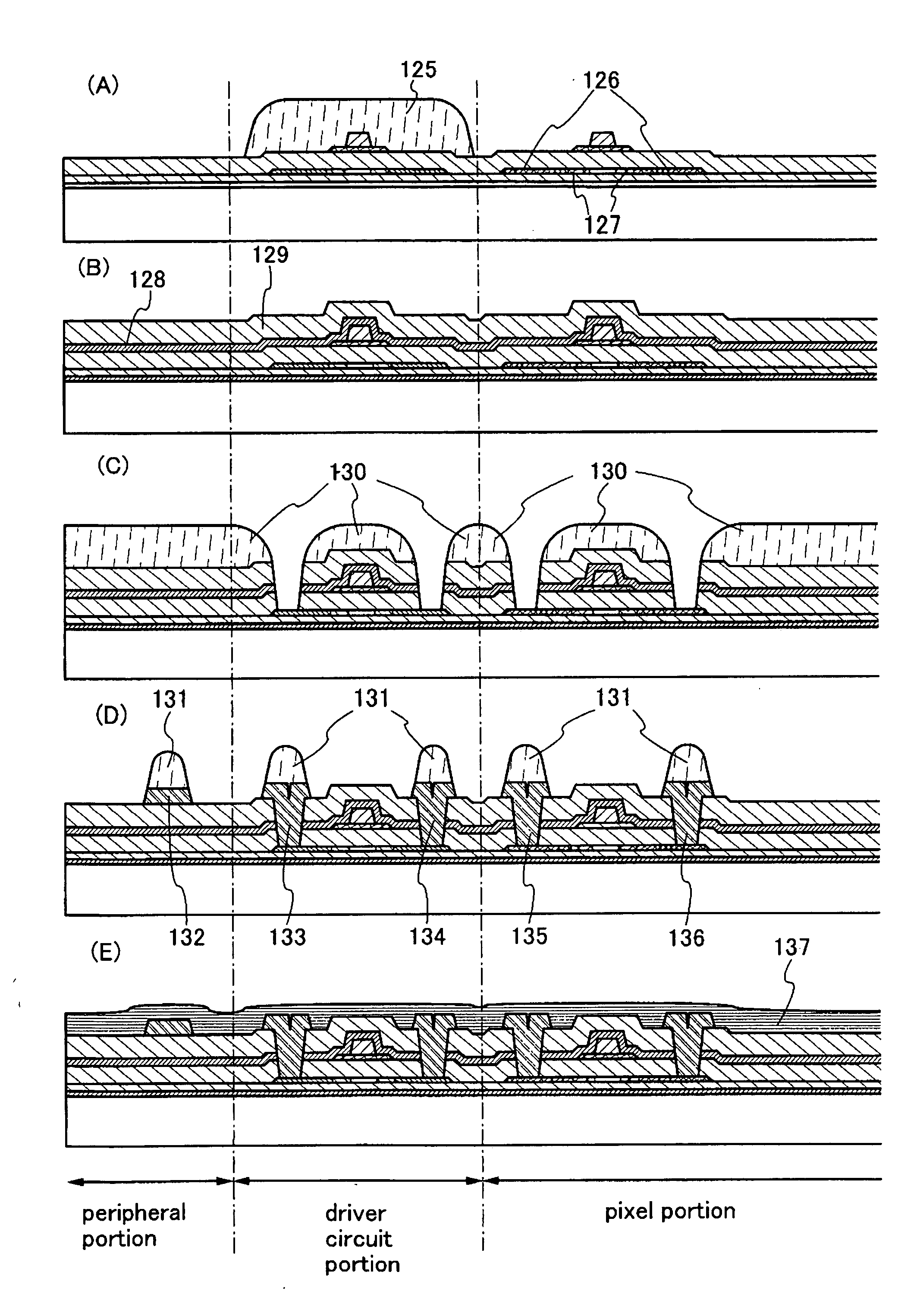
[0109] A method for manufacturing a display device of the present invention, which is different from that of Embodiment Mode 1, will be described with reference to FIGS. 5 and 6. The processing steps are halfway the same as those of Embodiment Mode 1; thus, the description and diagrams are omitted. Refer to Embodiment Mode 1. FIG. 5A corresponds to FIG. 2B.

[0110] After manufacturing up to the state shown in FIG. 5A following Embodiment Mode 1, a planarizing film 150 is formed to cover an interlayer insulating film 129 (FIG. 5B). As a material of the planarizing film 150, an application film with a self-planarizing property that can relieve unevenness formed in the lower layer by forming the film, for example, acrylic, polyimide, or siloxane is preferably used. That is, a material that can form a film having unevenness smaller than that formed in the lower layer can be publicly employed. In addition, a film of which unevenness is relieved by reflowing or polishing the film once form...

embodiment mode 3

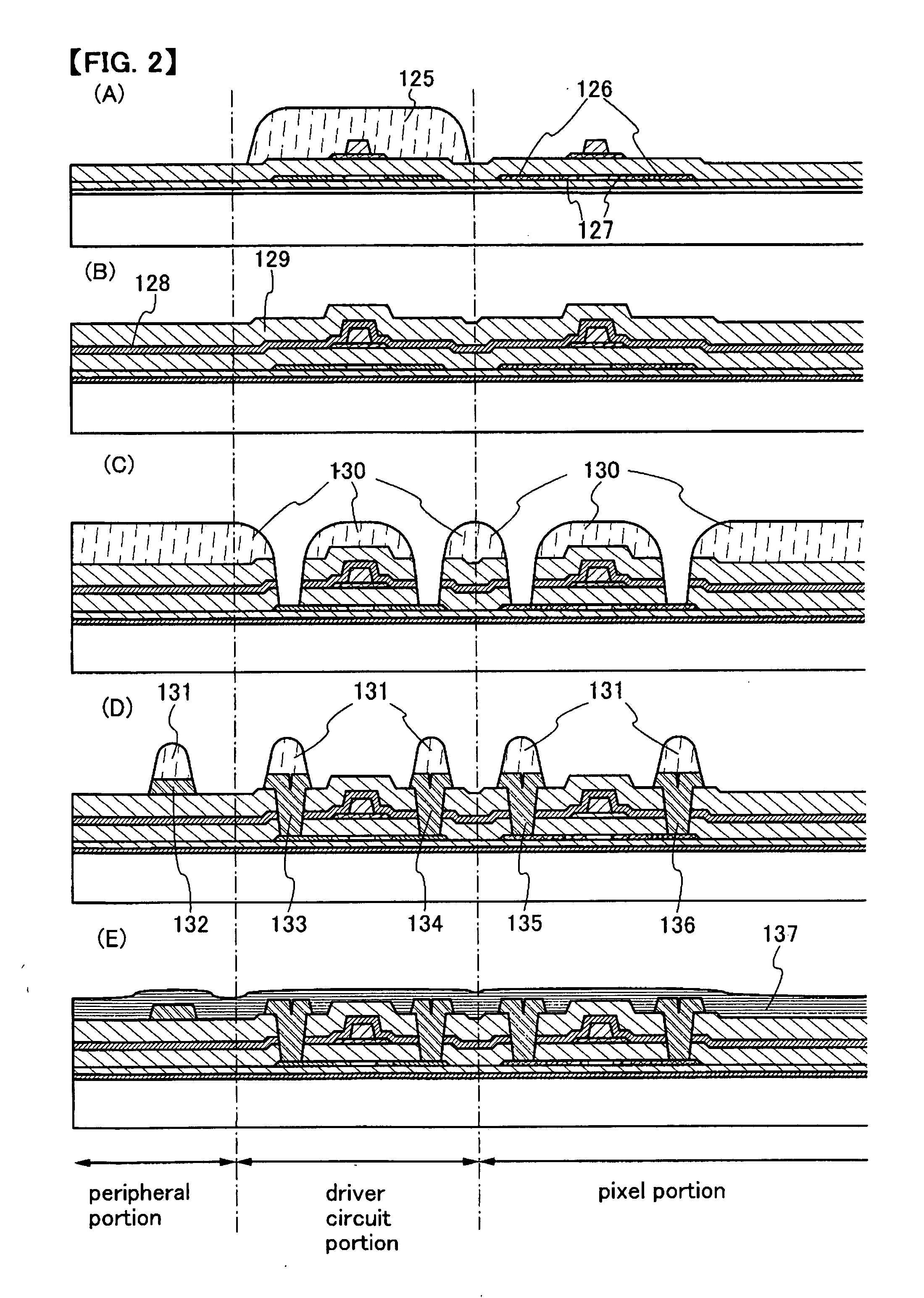
[0134] A method for manufacturing a display device of the present invention, which is different from those of Embodiment Modes 1 and 2, will be described with reference to FIGS. 7 and 8. The processing steps are halfway the same as those of Embodiment Mode 1; thus, the description and diagrams are omitted. Refer to Embodiment Mode 1. FIG. 7A corresponds to FIG. 2B.

[0135] After manufacturing up to the state shown in FIG. 7A following Embodiment Mode 1, a planarizing film 150 is formed to cover an interlayer insulating film 129 (FIG. 7B). As a material of the planarizing film 150, an application film with a self-planarizing property that can relieve unevenness formed in the lower layer by forming the film, for example, acrylic, polyimide, or siloxane is preferably used. That is, a material that can form a film having unevenness smaller than that formed in the lower layer can be publicly employed. In addition, a film of which unevenness is relieved by reflowing or polishing the film o...


PUM


Abstract

It is an object of the present invention to provide a method for manufacturing a display device in which unevenness generated under a light-emitting element does not impart an adverse effect on the light-emitting element. It is another object of the invention to provide a method for manufacturing a display device in which penetration of water into the inside of the display device through a film having high moisture permeability can be suppressed without increasing processing steps considerably. It is another object of the invention to provide a display device and a method for manufacturing a display device satisfying the above two simultaneously. A display device of the present invention to solve the above problems comprising a thin film transistor and a light-emitting element over an insulating surface formed on a substrate, wherein the light-emitting element includes a light-emitting laminated body interposed between a first electrode and a second electrode; wherein the first electrode is formed over an insulating film formed over the thin film transistor; and wherein a planarizing film is formed in response to the first electrode between the first electrode and the insulating film.

Description

BACKGROUND OF THE INVENTION [0001] The present invention relates to a method for manufacturing a display device using an element emitting light (light-emitting element) by applying current between electrodes interposing a light-emitting material therebetween. DESCRIPTION OF RELATED ART [0002] In recent years, a thin lightweight display using a light-emitting element has been actively developed. The light-emitting element is manufactured by interposing a material which emits light by applying current between a pair of electrodes. Since the light-emitting element itself emits light unlike in the case of liquid crystal, a light source such as a backlight is not required, and the element is very thin. Therefore, it is extremely advantageous to manufacture a thin lightweight display. [0003] However, one background of not reaching practical use yet while having such big advantages is a problem of reliability. The light-emitting element using an organic-based material often deteriorates du...

Claims


Application Information

Patent Timeline
Patent Type & Authority Applications(United States)
IPC IPC(8): H01L29/04H01L29/15H01L31/036
CPCG09G3/3225G09G3/3233G09G2300/0842G09G2300/0861G09G2310/0251G09G2310/0262H01L33/0041H01L27/3246H01L27/3248H01L27/3258H01L51/5246H01L51/56H01L27/3244H10K59/123H10K59/122H10K59/124H10K59/12H10K50/8426H10K71/00H01L27/1218H01L27/1248H01L29/78603H01L29/78636H01L29/78654
Inventor SAKAKURA, MASAYUKIYAMAZAKI, SHUNPEI
Owner SEMICON ENERGY LAB CO LTD
Why Eureka
Try Eureka