System and method for signal integrity testing of electronic circuits

a technology of electronic circuits and signal integrity testing, applied in error detection/correction, detecting faulty computer hardware, instruments, etc., can solve the problems of significant signal crosstalk or coupling noise, signal crosstalk and coupling noise problems are exacerbated in high speed and very large-scale circuit devices, and accurately identify one or more levels of coupling noise in the device involved.

Inactive Publication Date: 2006-08-24
HONEYWELL INT INC
View PDF8 Cites 9 Cited by
  • Summary
  • Abstract
  • Description
  • Claims
  • Application Information

AI Technical Summary

Benefits of technology

[0007] The present invention provides a system and method for measuring signal crosstalk in an electronic circuit, electronic circuit device or IC device, correlating the results with reference information, and accurately identifying one or more levels of coupling noise in the device involved. In a preferred embodiment, a system is used to provide data on the level(s) of crosstalk between conductive lines in a device. Also, the system uses multiple programmable victim and aggressor lines, programmable drive capability, and programmable loading through one or more known crosstalk structures to compare an output signal with a reference signal and accurately identify one or more levels of coupling noise in the device.

Problems solved by technology

In the design and manufacture of electronic circuit devices or IC devices including, for example, Application Specific IC (ASIC), Large-Scale IC (LSIC), or Very Large-Scale IC (VLSIC) devices, a significant problem encountered with such devices is that the input and output terminals of the logic circuit units (e.g., circuit cells, blocks, etc.) in the devices are interconnected with metallic wiring or other forms of conductive lines.
Consequently, the very high integration and mounting densities required of the circuit cells, blocks and wiring in such devices create significant levels of signal crosstalk or coupling noise.
Signal crosstalk and coupling noise are derived from signal interference in electronic circuit devices or IC devices, which is caused by the close proximities of the connecting wires or conductors throughout the device.
Also, signal crosstalk and coupling noise problems are exacerbated in high speed and very large-scale circuit devices.
Currently, levels of signal coupling between multiple layers of metal or other conductive materials in a circuit device can be difficult to quantify with any reasonable degree of accuracy.

Method used


Image

  • System and method for signal integrity testing of electronic circuits
  • System and method for signal integrity testing of electronic circuits
  • System and method for signal integrity testing of electronic circuits

Examples


Embodiment Construction

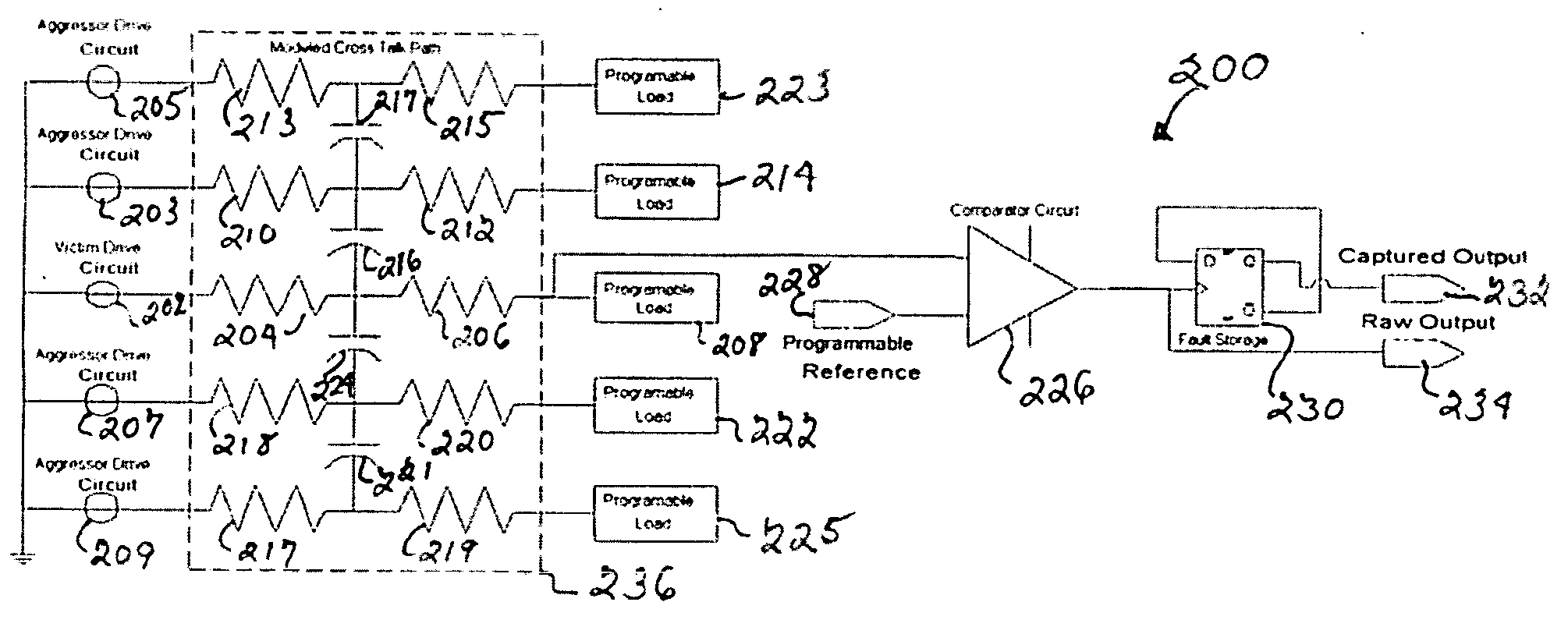
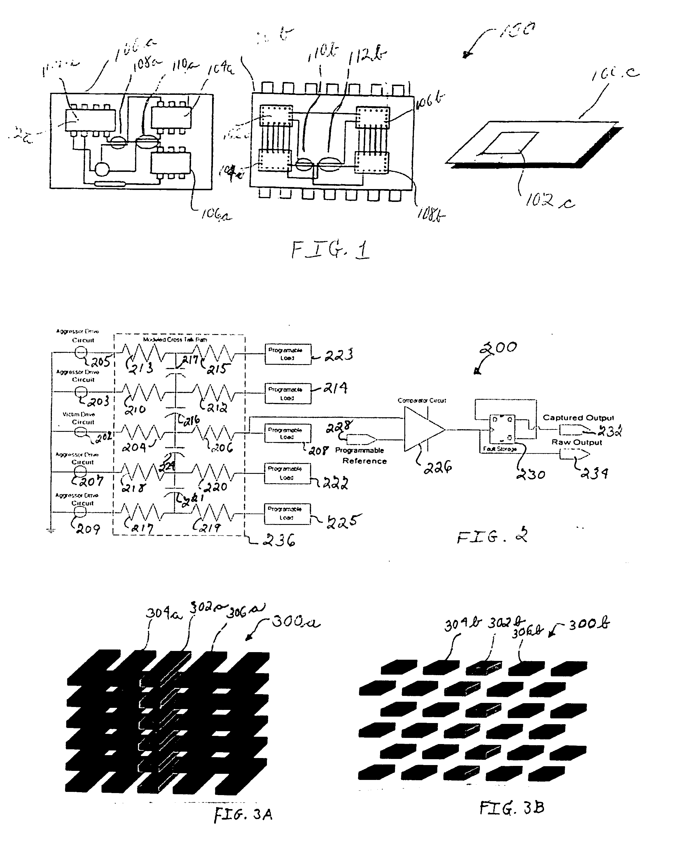
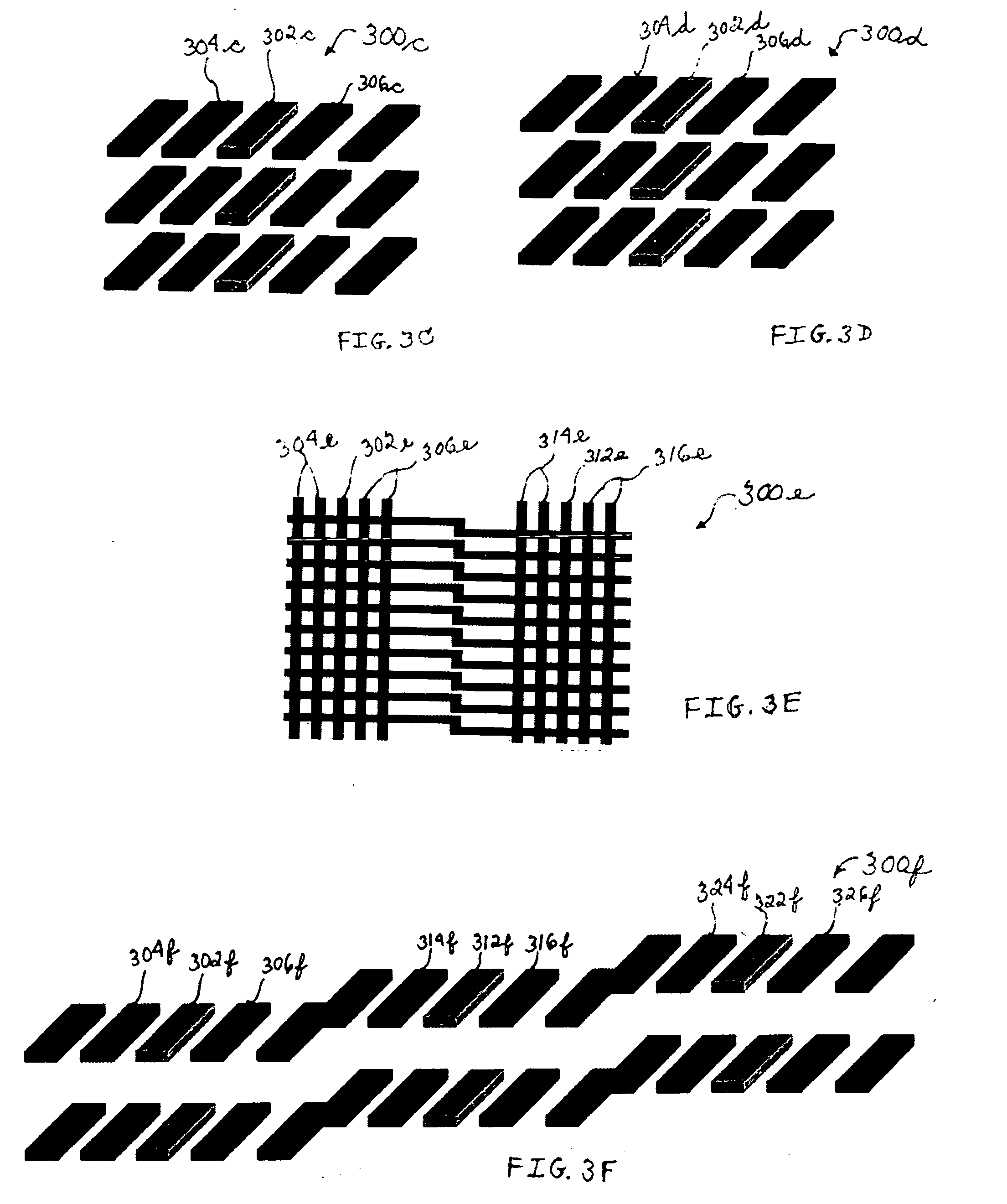
[0013] With reference now to the figures, FIG. 1 depicts a pictorial representation of a plurality of example electronic circuit layouts (or environments) 100a-100c, each of which may be used to implement one or more embodiments of the present invention. For example, electronic circuit layout 100a can represent a circuit board, which includes a plurality of electronic circuit devices 102a, 104a and 106a. Each electronic circuit device 102a, 104a and 106a can be, for example, a packaged semiconductor device (e.g., including one or more chips) providing one or more logical functions. As shown, at least one terminal of each electronic circuit device 102a, 104a and 106a is connected via a conductive wire or line to at least one terminal of another electronic circuit device 102a, 104a and 106a. Notably, at two areas or regions (e.g., indicated by the ellipses 108a, 110a) in electronic circuit layout 100a, two interconnecting conductive wires or lines are arranged in close proximity to ea...


PUM


Abstract

A system and method are disclosed for measuring signal crosstalk in an electronic circuit device or Integrated Circuit (IC) device, correlating the results with modeled information, and accurately identifying one or more levels of coupling noise in the device. For example, a system is disclosed that provides data on levels of crosstalk between conductive lines in a device. The system uses programmable victim and aggressor lines, programmable drive capability, and programmable loading through one or more known crosstalk structures to compare an output signal with a reference signal and accurately identify one or more levels of coupling noise in the device. An external reference signal can be used to detect upsets or crosstalk in the device. As such, using such programmability features of the system, numerous combinations of coupling in a device can be measured at a time. For example, one or more lines in the device can be programmed to represent victim lines, while other lines in the device can be programmed to represent aggressor lines. An output signal of the system can be compared to a known signal. For example, a DC offset voltage can be used to determine an exact level of upset or crosstalk that exists in the device. Alternatively, an AC clocking signal can be used to measure timing push-out or edge degradation in the device.

Description

GOVERNMENT LICENSE RIGHTS [0001] The U.S. Government may have certain rights in the present invention as provided for by the terms of Contract No. DTRA01-02-D-0008 awarded by the Defense Threat Reduction Agency.BACKGROUND OF THE INVENTION [0002] 1. Technical Field [0003] The present invention relates generally to the electronic circuit test field, and more particularly, but not exclusively, to a system and method for programmable signal integrity testing to identify levels of coupling noise in an electronic circuit such as, for example, a packaged electronic circuit device or semiconductor Integrated Circuit (IC) device. [0004] 2. Description of Related Art [0005] In the design and manufacture of electronic circuit devices or IC devices including, for example, Application Specific IC (ASIC), Large-Scale IC (LSIC), or Very Large-Scale IC (VLSIC) devices, a significant problem encountered with such devices is that the input and output terminals of the logic circuit units (e.g., circui...

Claims


Application Information

Patent Timeline
Patent Type & Authority Applications(United States)
IPC IPC(8): G06F17/50
CPCG01R31/31813G01R31/318371G01R31/31917G01R31/31932
Inventor CRESS, DAVID S.
Owner HONEYWELL INT INC
Why Eureka
Try Eureka