Methods and systems for electroplating wafers

a technology of electroplating wafers and substrates, applied in the field of electroplating substrate methods and systems, can solve the problems of large amount of time and labor for plating solution analysis and control, severe penalization of the overall performance of the structure, etc., and achieve the effects of reducing the production rate of breakdown products produced during electroplating, reducing the useable life of plating solution, and reducing the consumption rate of additives enhancing electroplating properties

Inactive Publication Date: 2006-08-31
HITACHI GLOBAL STORAGE TECH NETHERLANDS BV
View PDF11 Cites 12 Cited by
  • Summary
  • Abstract
  • Description
  • Claims
  • Application Information

AI Technical Summary

Benefits of technology

[0014] By stopping the flow of plating solution after completion of plating one or more wafers, a consumption rate of additives enhancing electroplating properties is reduced, a production rate of breakdown products produced during electroplating is reduced, plating solution useable life is increased, and a need for plating solution analysis is reduced.

Problems solved by technology

The trend to smaller chip sizes and increased circuit density requires the miniaturization of interconnect features which severely penalizes the overall performance of the structure because of increasing interconnect resistance and reliability concerns such as fabrication of the interconnects and electromigration.
Both of these requirements result in a large amount of time and labor for plating solution analysis and control.

Method used


Image

  • Methods and systems for electroplating wafers
  • Methods and systems for electroplating wafers
  • Methods and systems for electroplating wafers

Examples


Embodiment Construction

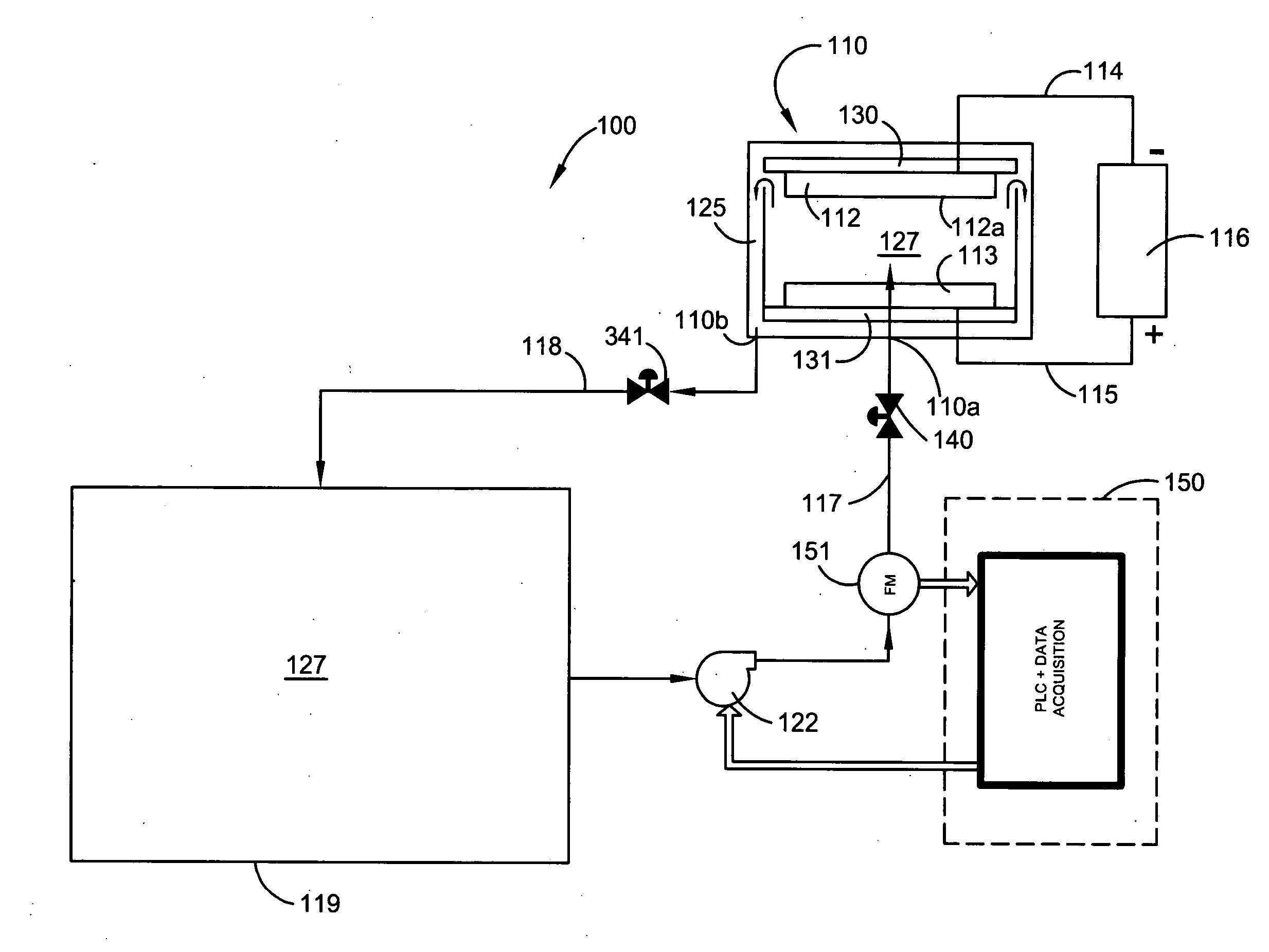
[0020] In describing the preferred embodiment of the present invention, reference will be made herein to FIGS. 1-4 of the drawings in which like numerals refer to like features of the invention. Features of the invention are not necessarily shown to scale in the drawings.

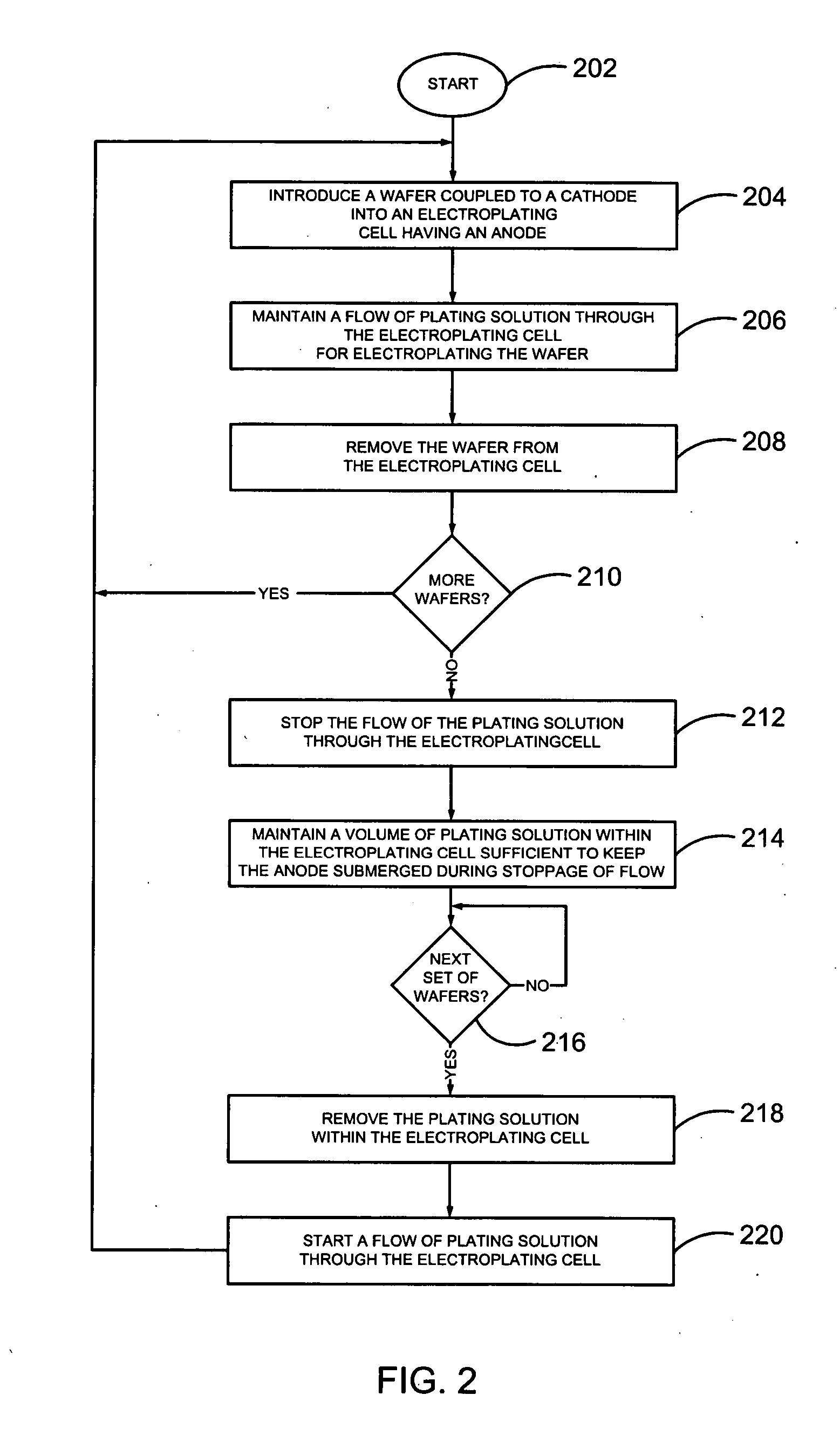
[0021]FIG. 2 is a flowchart which describes an improved method for electroplating wafers in accordance with the present invention. FIGS. 3-4 are process flow diagrams of plating systems 300 and 400 of the present invention within which the steps in the flowchart of FIG. 2 may be employed. While the systems and methods are described primarily with reference to plating a silicon wafer, it will be appreciated by those skilled in the art that other substrates may be plated. Although any suitable system platform may be utilized, the plating system may be based on the type provided by Semitool, Inc. of Kalispell, Mont., U.S.A., for example, the EQUINOX® system platform (EQUINOX is a registered trademark of Semitool, Inc....


PUM

PropertyMeasurementUnit
concentrationaaaaaaaaaa
time periodaaaaaaaaaa

Abstract

Improved methods and systems for electroplating wafers are described herein. The method includes the acts of introducing a wafer which is coupled to an electrode into an electroplating cell having a counter electrode; maintaining a flow of a plating solution through the cell for electroplating the wafer; removing the wafer from the cell; stopping the flow of the plating solution through the cell; maintaining a volume of plating solution within the cell sufficient to keep the counter electrode submerged during stoppage of flow; removing the plating solution within the cell; and repeating the above steps for a subsequent wafer. By stopping the flow of plating solution after completion of plating one or more wafers, a consumption rate of additives enhancing electroplating properties is reduced, a production rate of breakdown products produced during electroplating is reduced, plating solution useable life is increased, and a need for plating solution analysis is reduced.

Description

BACKGROUND OF THE INVENTION [0001] 1. Field of the Invention [0002] This invention relates generally to methods and systems for electroplating substrates, such as those utilized for damascene electroplating of write coils in magnetic heads. [0003] 2. Description of the Related Art [0004] The demand for manufacturing semiconductor integrated circuit (IC) devices, such as computer chips with high circuit speed, high-packing density, and low power dissipation, requires the downward scaling of feature sizes in ultra-large-scale integration (ULSI) and very-large-scale integration (VLSI) structures. The trend to smaller chip sizes and increased circuit density requires the miniaturization of interconnect features which severely penalizes the overall performance of the structure because of increasing interconnect resistance and reliability concerns such as fabrication of the interconnects and electromigration. Magnetic heads with inductive write coils also feature miniaturization requireme...

Claims


Application Information

Patent Timeline
Patent Type & Authority Applications(United States)
IPC IPC(8): C25D17/00C25D5/20C25D5/02
CPCC25D3/38C25D21/12H01L21/2885C25D5/08C25D17/001
Inventor HITZFELD, ROBERT WILLIAMLOO, JENNIFER AI-MINGRAMASUBRAMANIAN, MURALI
Owner HITACHI GLOBAL STORAGE TECH NETHERLANDS BV
Why Eureka
Try Eureka