Passive component

a passive component and component technology, applied in the direction of resonators, electrical equipment, waveguides, etc., to achieve the effect of effectively simplifying manufacturing steps and effectively reducing character variations

Active Publication Date: 2006-08-31
SOSHIN ELECTRIC
View PDF11 Cites 20 Cited by
  • Summary
  • Abstract
  • Description
  • Claims
  • Application Information

AI Technical Summary

Benefits of technology

[0025] As described above, the passive component according to the present invention can solve various problems caused by side mounting, characteristic variations can effectively be reduced, and manufacturing steps can effectively be simplified.

Problems solved by technology

However, the above side mounting suffers the following problems:

Method used


Image

  • Passive component
  • Passive component
  • Passive component

Examples


first embodiment

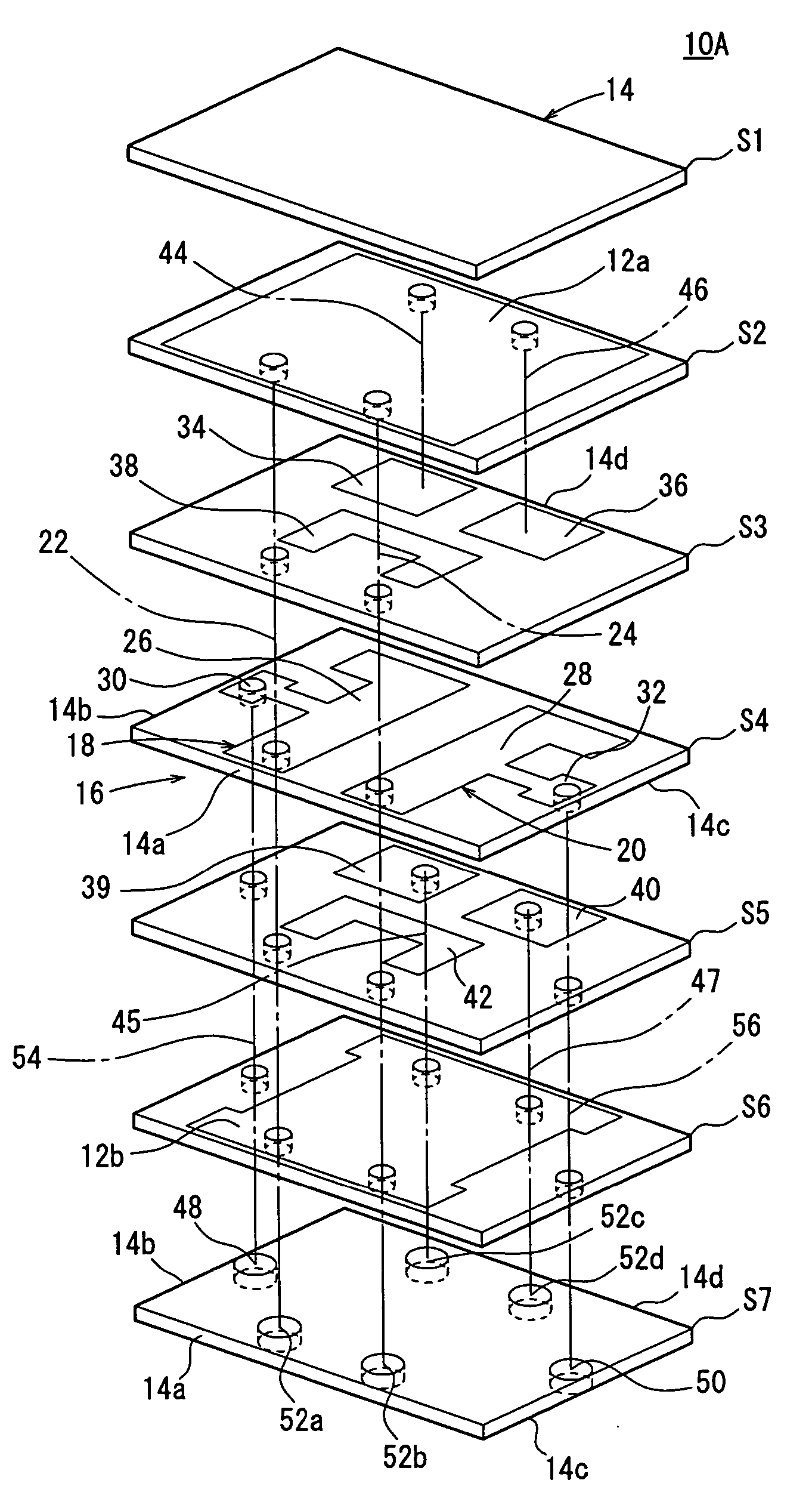
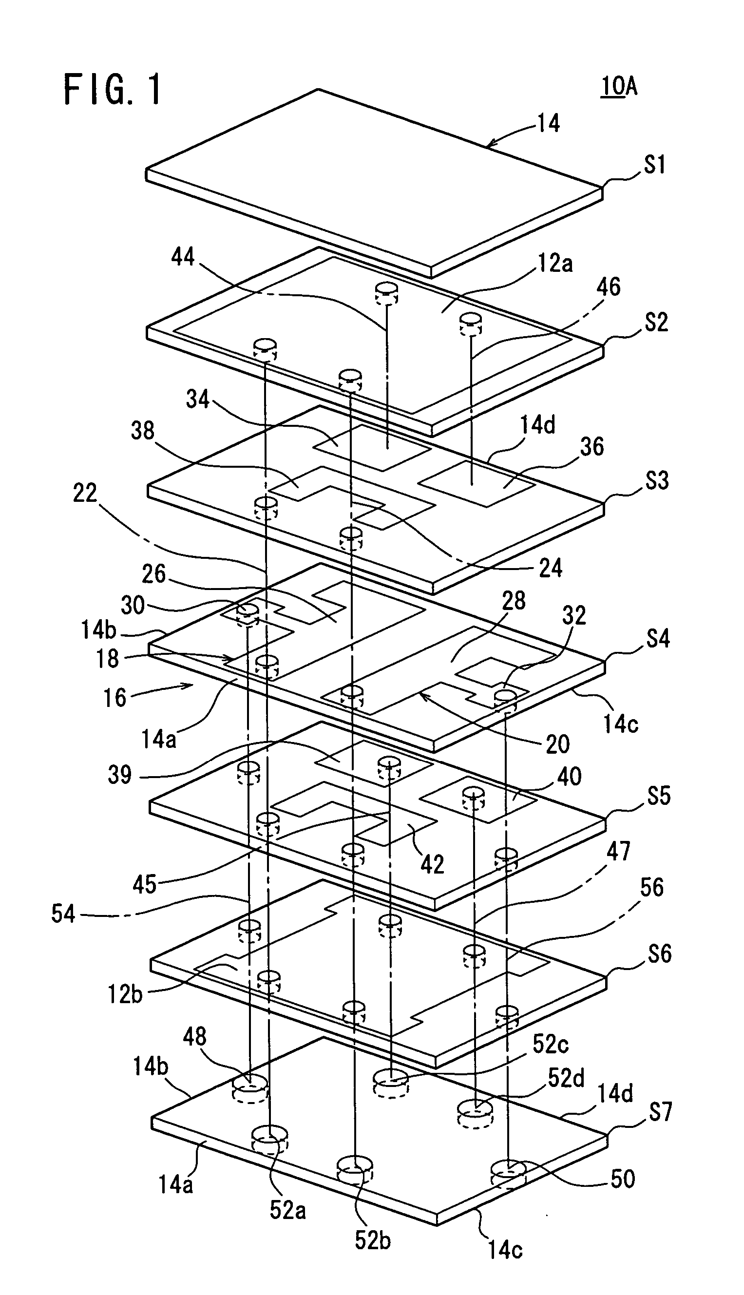
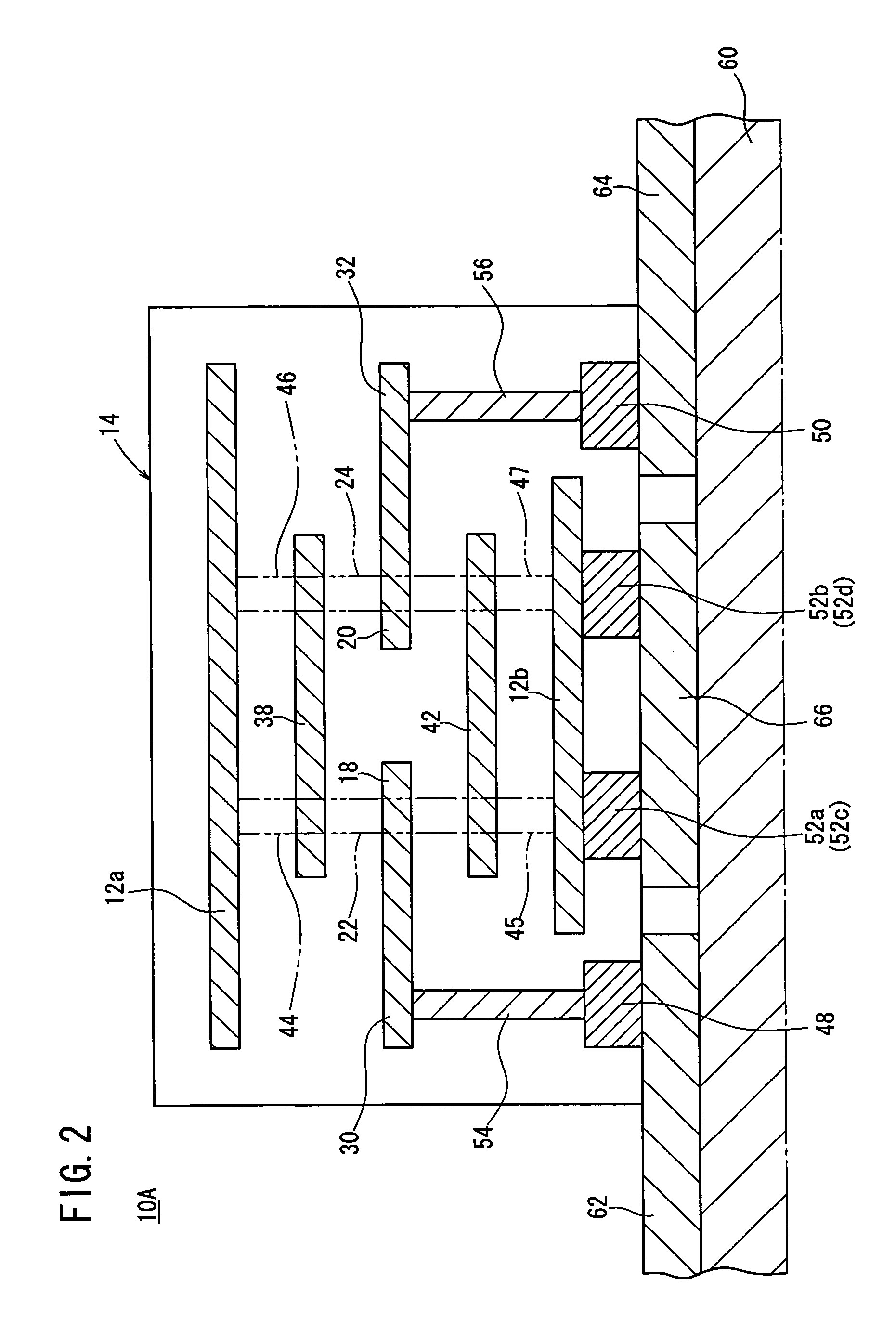
[0035] As shown in FIGS. 1 and 2, a passive component 10A has a dielectric substrate 14 including a plurality of dielectric layers (S1 through S7) stacked and sintered together and inner-layer shield electrodes 12a, 12b disposed respectively on both principal surfaces (a principal surface of the second dielectric layer S2 and a principal surface of the sixth dielectric layer S6).

[0036] The dielectric substrate 14 is constructed by successively stacking the first through seventh dielectric layers S1 through S7. Each of the first through seventh dielectric layers S1 through S7 comprises a single layer or a plurality of layers.

[0037] The dielectric substrate 14 includes a filter 16 providing two ¼-wavelength resonators (an input resonator 18 and an output resonator 20). The filter 16 has an input resonant electrode 26 and an output resonant electrode 28 which are disposed on a principal surface of the fourth dielectric layer S4.

[0038] An end of the input resonant electrode 26 (an en...

second embodiment

[0056] A passive component 10B will be described below with reference to FIGS. 3 and 4.

[0057] As shown in FIGS. 3 and 4, the passive component 10B according to the second embodiment is of essentially the same structure as the passive component 10A according to the first embodiment, but differs therefrom in that the input resonator 18 and the output resonator 20 are constructed of via holes 70, 72.

[0058] Specifically, as shown in FIG. 3, the input resonator 18 has a first electrode 74 extending on a principal surface of the third dielectric layer S3 from a region close to the first side surface 14a to a region close to the fourth side surface 14d, a second electrode 76 extending on a principal surface of the fifth dielectric layer S5 from a region close to the first side surface 14a to a region close to the fourth side surface 14d, and a via hole 70, referred to above, extending through the third and fourth dielectric layers S3, S4 and interconnecting a central portion of the first...

third embodiment

[0073] A passive component 10C will be described below with reference to FIG. 5.

[0074] As shown in FIG. 5, the passive component 10C according to the third embodiment is of essentially the same structure as the passive component 10B according to the second embodiment, but differs therefrom in that the shield electrode films 96, 98 (see FIG. 3) are not disposed on the lower surface of the dielectric substrate 14, and, of the dielectric layers S1 through S7 that make up the dielectric substrate 14, the sixth and seventh dielectric layers S6, S7 between the inner-layer shield electrode 12b and the lower surface of the dielectric substrate 14 are made of a material having a dielectric constant εr (>20).

[0075] The inner-layer shield electrode 12b in the dielectric substrate 14 and the shield wiring pattern 66 on the wiring board 60 can be electrically connected to each other through a capacitance.

[0076] Therefore, the shield electrode films 96, 98 (see FIG. 3) serving as the shield te...


PUM


Abstract

A passive component comprising one input electrode layer constituting an input terminal, one output electrode layer constituting an output terminal, and four shield electrode layers constituting shield terminals, all formed in the lowermost dielectric layer by via holes. The input electrode layer is connected electrically with an input-side resonance electrode, in the vicinity of the second side face of a dielectric substrate, through a via hole made in the fourth through sixth dielectric layers and an input tap electrode. The output electrode layer is connected electrically with an output-side resonance electrode, in the vicinity of the third side face of the dielectric substrate, through a via hole made in the fourth through sixth dielectric layers and an output tap electrode.

Description

TECHNICAL FIELD [0001] The present invention relates to a passive component such as a multilayered dielectric filter for resonant circuits for use in a microwave band ranging from several hundred MHz to several GHz, and more particularly to a passive component which is effective in making communication devices and electronic devices small in size. BACKGROUND ART [0002] Recently, ICs have been highly integrated and fast becoming smaller in size. Passive components such as filters for use with ICs have also become smaller in size. Multilayered dielectric passive components employing dielectric substrates are effective in making passive components smaller in size (see, for example, Japanese Laid-Open Patent Publication No. 2002-280805 and Japanese Laid-Open Patent Publication No. 2002-261643). [0003] When a multilayered dielectric passive component is mounted on a wiring board, for example, a wiring pattern disposed on the wiring board and input and output terminals disposed on sides o...

Claims


Application Information

Patent Timeline
Patent Type & Authority Applications(United States)
IPC IPC(8): H01P1/203H01P1/205H01P5/10H03H7/075H03H7/42
CPCH01P1/20345H01P1/203H01P1/205
Inventor URANO, MASAKIHIRAI, TAKAMIMIZUTANI, YASUHIKOTAKASE, KOUHEI
Owner SOSHIN ELECTRIC
Why Eureka
Try Eureka