Pattern transferring apparatus and pattern transferring method
- Summary
- Abstract
- Description
- Claims
- Application Information
AI Technical Summary
Benefits of technology
Problems solved by technology
Method used
Image

Examples
embodiment 1
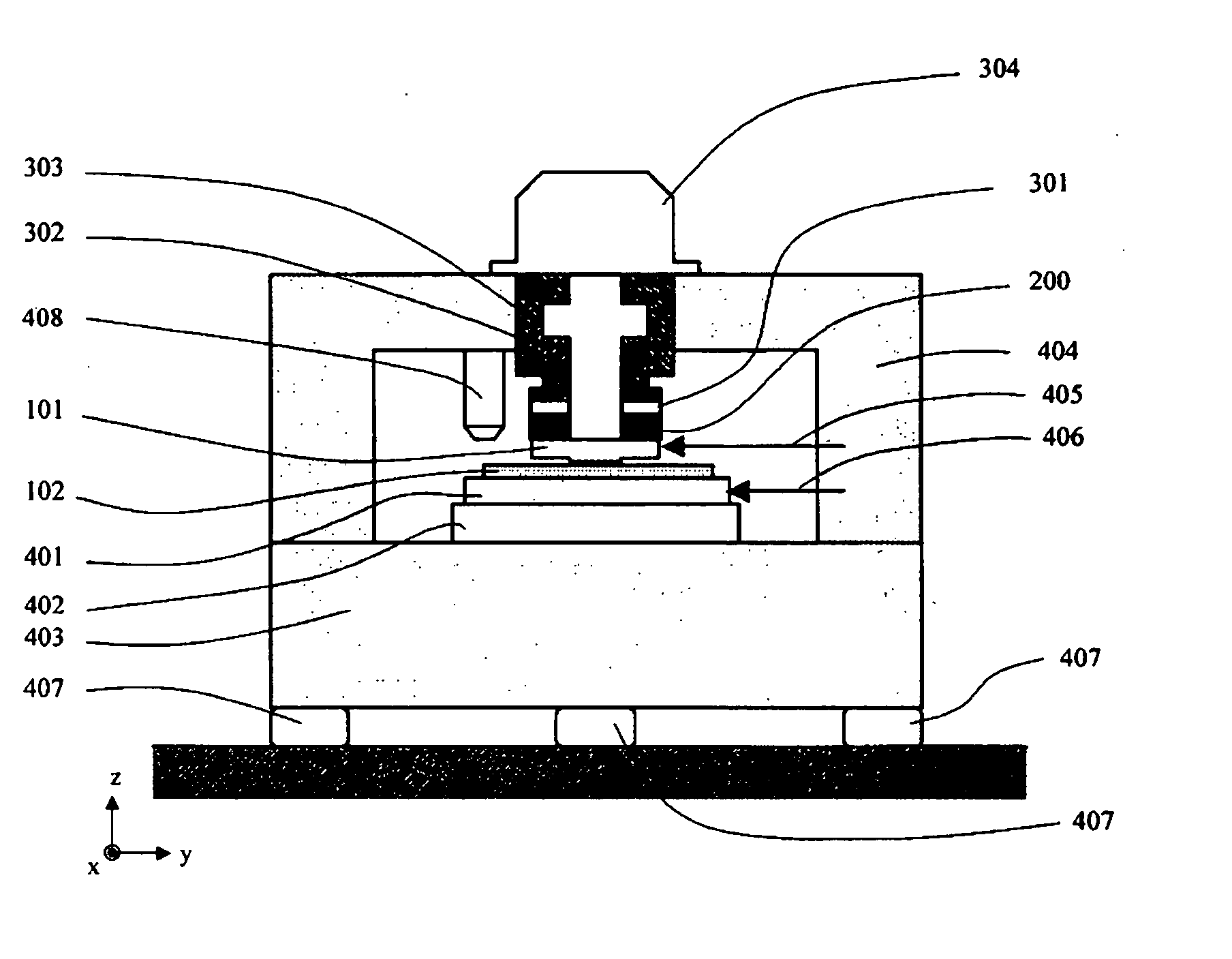
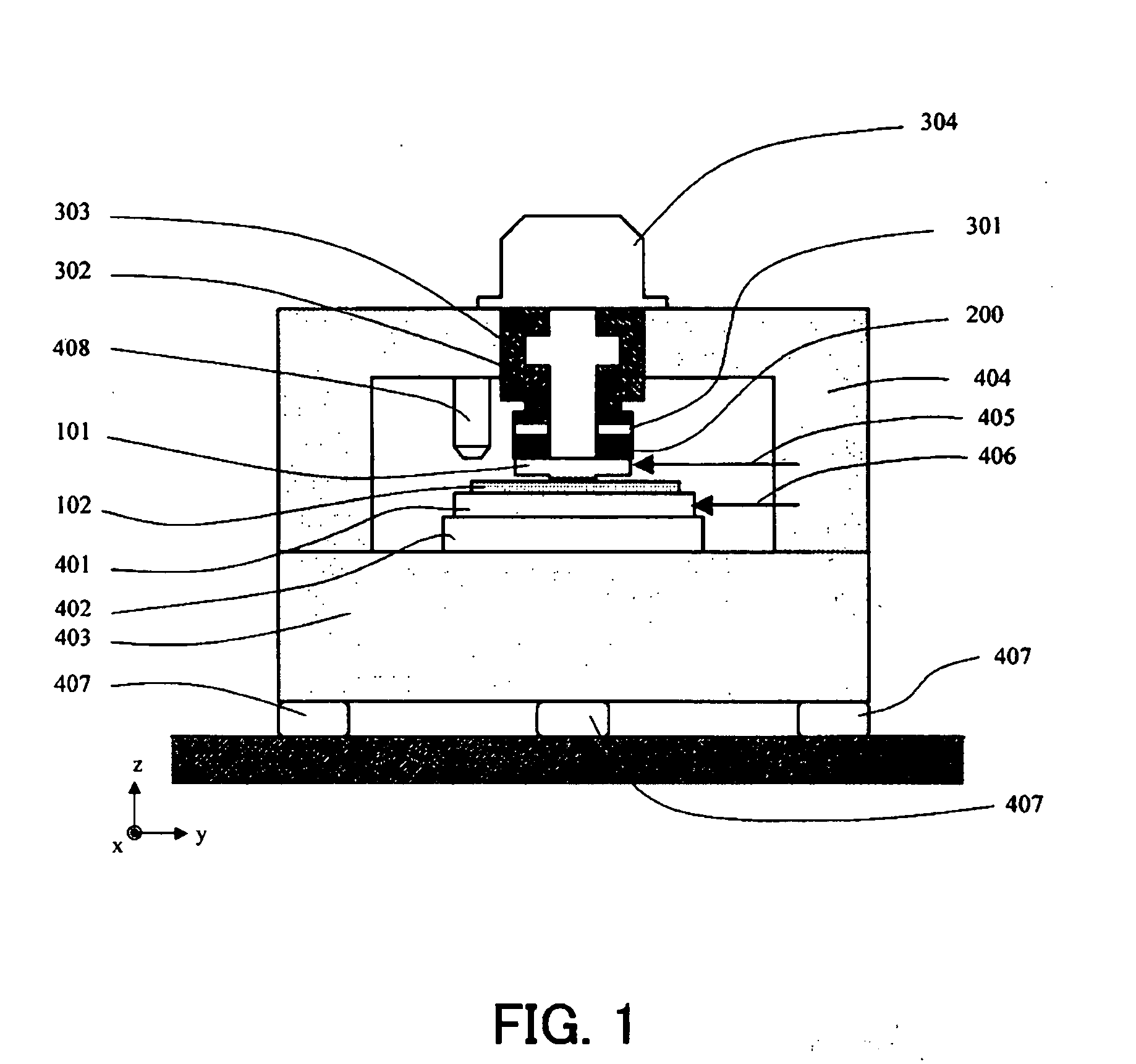
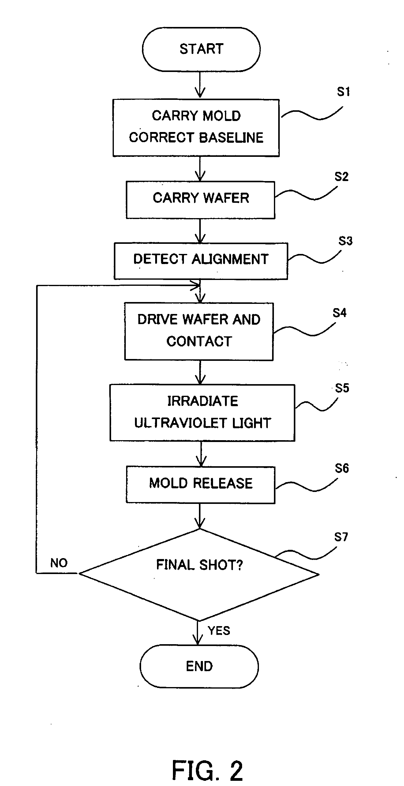
[0037]FIG. 1 shows a UV-curing nanoimprint lithography apparatus (hereinafter referred to simply as a nanoimprint apparatus) serving as a pattern transferring apparatus which is Embodiment 1 of the present invention. The nanoimprint apparatus is of a step and repeat type in which a mold having a circuit pattern for a single or a plurality of chips of a semiconductor device formed thereon is successively transferred onto a resist made of UV-curing resin applied to a wafer.
[0038] In FIG. 1, reference numeral 101 shows a mold (also referred to as an original plate, a template or the like) made of a material which passes ultraviolet light, for example, quartz. A pattern corresponding to the abovementioned circuit pattern is formed three-dimensionally on the bottom of the mold 101. The area of the mold 101 that has the pattern formed thereon will hereinafter be referred to as a pattern area or a pattern surface.
[0039] Reference numeral 102 shows a wafer which is a substrate to be proce...
embodiment 2
[0065]FIG. 7 shows the structure of part of a nanoimprint apparatus which is Embodiment 2 of the present invention, including components from a mold stage 301 to a wafer 102. In Embodiment 2, the components having the same functions as those in Embodiment 1 are designated with the same reference numerals as in Embodiment 1 and description thereof is omitted.
[0066] Reference numeral 200A shows a mold chuck of the nanoimprint apparatus. The mold chuck 200A holds a mold 101 and also has the function of forming a starting point of mold release at the time of mold release, as later described. The surface of the mold 101 opposite to a pattern surface (that is, the top surface) serves as a reference plane for positioning.
[0067] The top surface of the mold 101 abuts on butt portions 208 provided at three positions in the mold chuck 200A opposite to that top surface, and the mold 101 is sandwiched between indenters 205L and 205R abutting on both sides of the mold 101, thereby retaining (ho...
embodiment 3
[0075]FIG. 8 shows the structure of part of a nanoimprint apparatus which is Embodiment 3 of the present invention, including components from a mold stage 301 to a wafer 102. In Embodiment 3, the components having the same functions as those in Embodiment 1 are designated with the same reference numerals as in Embodiment 1, and description thereof is omitted.
[0076] Reference numeral 200B shows a mold chuck. The top surface of the mold 101 abuts on butt portions 507 formed in the mold chuck 200B in a Z direction, and the right surface of the mold 101 abuts on a butt portion 505 in an XY direction, thereby positioning the mold 101 with respect to the apparatus at a predetermined position and a predetermined attitude.
[0077] In addition, the mold 101 is held from below at both ends on the left and right by mold securers 506 provided for the mold chuck 200B to retain the mold 101 by the mold chuck 200B.
[0078] Reference numeral 501 shows an infrared light source which is fixed to the m...
PUM
| Property | Measurement | Unit |
|---|---|---|
| Temperature | aaaaa | aaaaa |
| Force | aaaaa | aaaaa |
| Area | aaaaa | aaaaa |
Abstract
Description
Claims
Application Information
 - Generate Ideas
- Intellectual Property
- Life Sciences
- Materials
- Tech Scout
- Unparalleled Data Quality
- Higher Quality Content
- 60% Fewer Hallucinations
Browse by: Latest US Patents, China's latest patents, Technical Efficacy Thesaurus, Application Domain, Technology Topic, Popular Technical Reports.
© 2025 PatSnap. All rights reserved.Legal|Privacy policy|Modern Slavery Act Transparency Statement|Sitemap|About US| Contact US: help@patsnap.com