Nanotube ESD protective devices and corresponding nonvolatile and volatile nanotube switches

a technology of nanotubes and nanotubes, applied in the direction of circuit electrostatic discharge protection, semiconductor/solid-state device details, instruments, etc., can solve the problems of resistor rupture, open circuit and short circuit, oxide and junction failure,

Inactive Publication Date: 2006-08-31
NANTERO
View PDF99 Cites 115 Cited by
  • Summary
  • Abstract
  • Description
  • Claims
  • Application Information

AI Technical Summary

Benefits of technology

[0018] Under another aspect of the invention, the nanotube switch prov

Problems solved by technology

Electrical overstress resulting from electrostatic discharge (ESD) is a major problem in every generation of electronic devices, resulting in oxide and junction failures such as series resistor rupture, open circuits and short circuits, for example.
Conventional resistors fabricated using polysilicon or diffusi

Method used


Image

  • Nanotube ESD protective devices and corresponding nonvolatile and volatile nanotube switches
  • Nanotube ESD protective devices and corresponding nonvolatile and volatile nanotube switches
  • Nanotube ESD protective devices and corresponding nonvolatile and volatile nanotube switches

Examples


Embodiment Construction

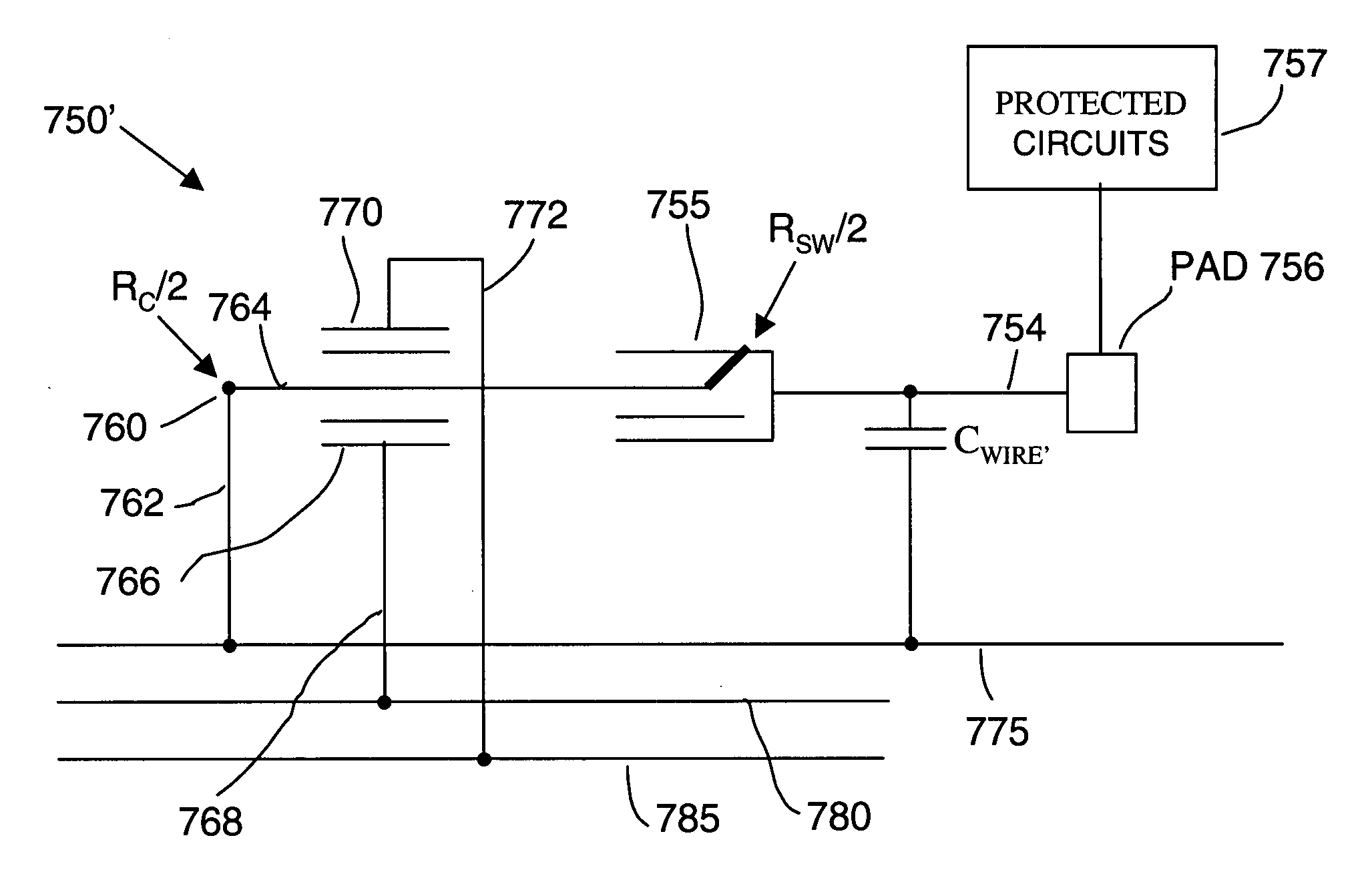
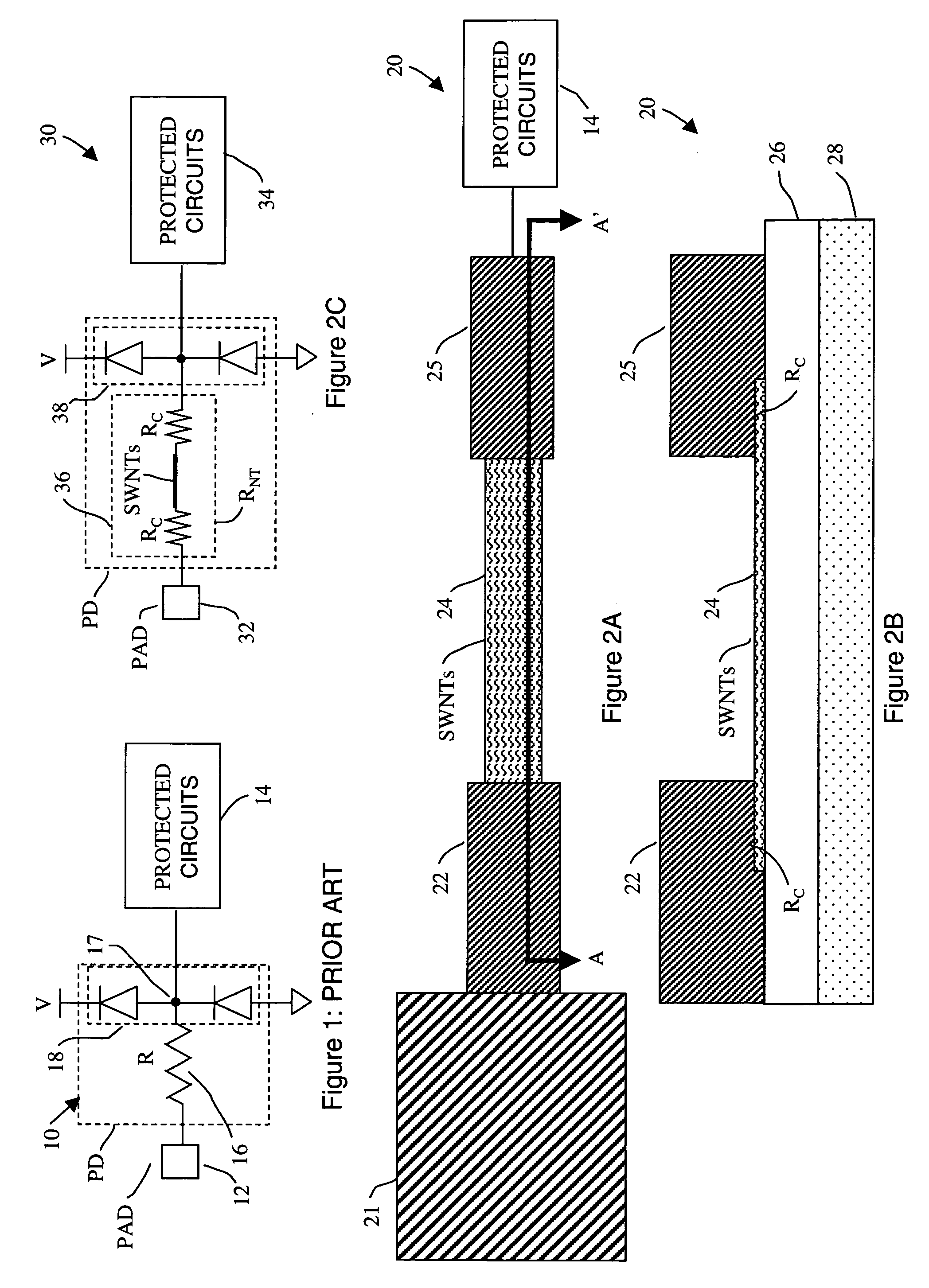
[0090] Non-volatile carbon nanotube protective devices offer an opportunity to enhance present electronic device protection by adding non-volatile carbon nanotube protective devices to prior art protective devices that require protective diodes as part of their structures. Nonvolatile nanotube protective device structures have much lower accompanying capacitance values than presently used protective devices, so that adding nonvolatile nanotube protective devices to existing electronic protective devices will not measurably increase capacitive loading. Capacitive loading by present protective devices introduces performance limitations, so that replacing these devices with non-volatile carbon nanotube protective devices reduces capacitive loading of inputs and outputs facilitating higher operating speeds. Carbon nanotube protective devices may be used on any substrate, such as silicon, ceramic, organic, etc. and may therefore be added at any level of assembly such as chip, substrate, ...


PUM

PropertyMeasurementUnit
Electric impedanceaaaaaaaaaa

Abstract

Nanotube ESD protective devices and corresponding nonvolatile and volatile nanotube switches. An electrostatic discharge (ESD) protection circuit for protecting a protected circuit is coupled to an input pad. The ESD circuit includes a nanotube switch electrically having a control. The switch is coupled to the protected circuit and to a discharge path. The nanotube switch is controllable, in response to electrical stimulation of the control, between a de-activated state and an activated state. The activated state creates a current path so that a signal on the input pad flows to the discharge path to cause the signal at the input pad to remain within a predefined operable range for the protected circuit. The nanotube switch, the input pad, and the protected circuit may be on a semiconductor chip. The nanotube switch may be on a chip carrier. The deactivated and activated states may be volatile or non-volatile depending on the embodiment. The ESD circuit may be repeatedly programmed between the activated and deactivated states so as to repeatedly activate and deactivate ESD protection of the protected circuit. The nanotube switch provides protection based on the magnitude of the signal on the input pad.

Description

CROSS-REFERENCE TO RELATED APPLICATION [0001] This application claims priority under 35 U.S.C. § 19(e) to the following applications, the contents of which are incorporated herein in their entirety by reference: [0002] U.S. Provisional Patent Application No. 60 / 624,428, filed on Nov. 2, 2004, entitled Nonvolatile Carbon Nanotube Protective Devices (NV-NT-PDs); and [0003] U.S. Provisional Patent Application No. 60 / 624,297, filed on Nov. 2, 2004, entitled Enhanced CNT Switching Operation.BACKGROUND [0004] 1. Technical Field [0005] The present application generally relates to ESD protections and, more specifically, to the use of nanotube switching elements in the formation of circuits for enhanced electrostatic discharge (EDS) protection of semiconductor, hybrid semiconductor and nanotube, and nanotube-only circuits. [0006] 2. Discussion of Related Art [0007] Electrical overstress resulting from electrostatic discharge (ESD) is a major problem in every generation of electronic devices,...

Claims


Application Information

Patent Timeline
IPC IPC(8): H02H9/00
CPCH01L2924/19103Y10T29/49124H01L2924/19105H01L2924/3011H05K1/0259B82Y10/00G11C13/025G11C17/16G11C17/165G11C23/00G11C2213/17H01H1/0094H01L23/60H01L23/62H01L27/0248H01L27/0251H01L51/0048H01L2224/16H01L2924/0102H01L2924/01025H01L2924/01046H01L2924/01077H01L2924/01079H01L2924/09701H01L2924/12044H01L2924/01019H01L2924/01066H01L2924/01068Y10T29/49204Y10T29/49105Y10T29/49117H01L2924/19104H10K85/221
Inventor BERTIN, CLAUDE L.SEGAL, BRENT M.RUECKES, THOMASWARD, JONATHAN W.
Owner NANTERO
Why Eureka
Try Eureka