Magnetoresistive element and magnetic memory device
a magnetic memory device and magnetoresistive element technology, applied in semiconductor devices, digital storage, instruments, etc., can solve the problems of low writing efficiency, low writing efficiency, and poor writing efficiency of mram, and achieve the effect of low writing efficiency
- Summary
- Abstract
- Description
- Claims
- Application Information
AI Technical Summary
Benefits of technology
Problems solved by technology
Method used
Image
Examples
Embodiment Construction
[0035] Hereinafter, an embodiment of the present invention will be described in detail with reference to the drawings.
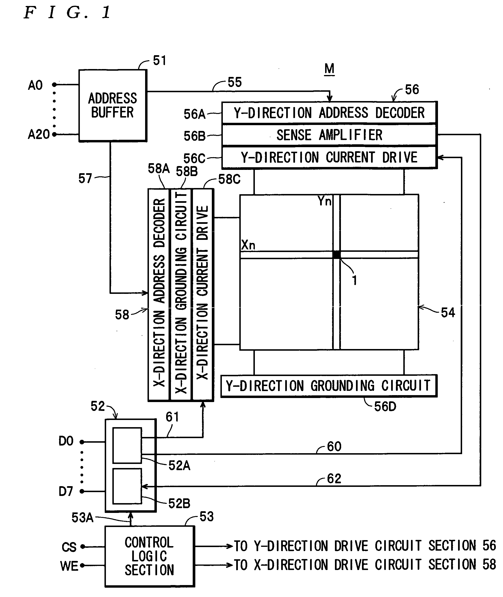
[0036] Referring first to FIG. 1, a description will be given of the construction of a magnetic memory device M.
[0037] The magnetic memory device M is comprised of an address buffer 51, a data buffer 52, a control logic section 53, a storage cell group 54, a Y-direction drive circuit section 56, and an X-direction drive circuit section 58.
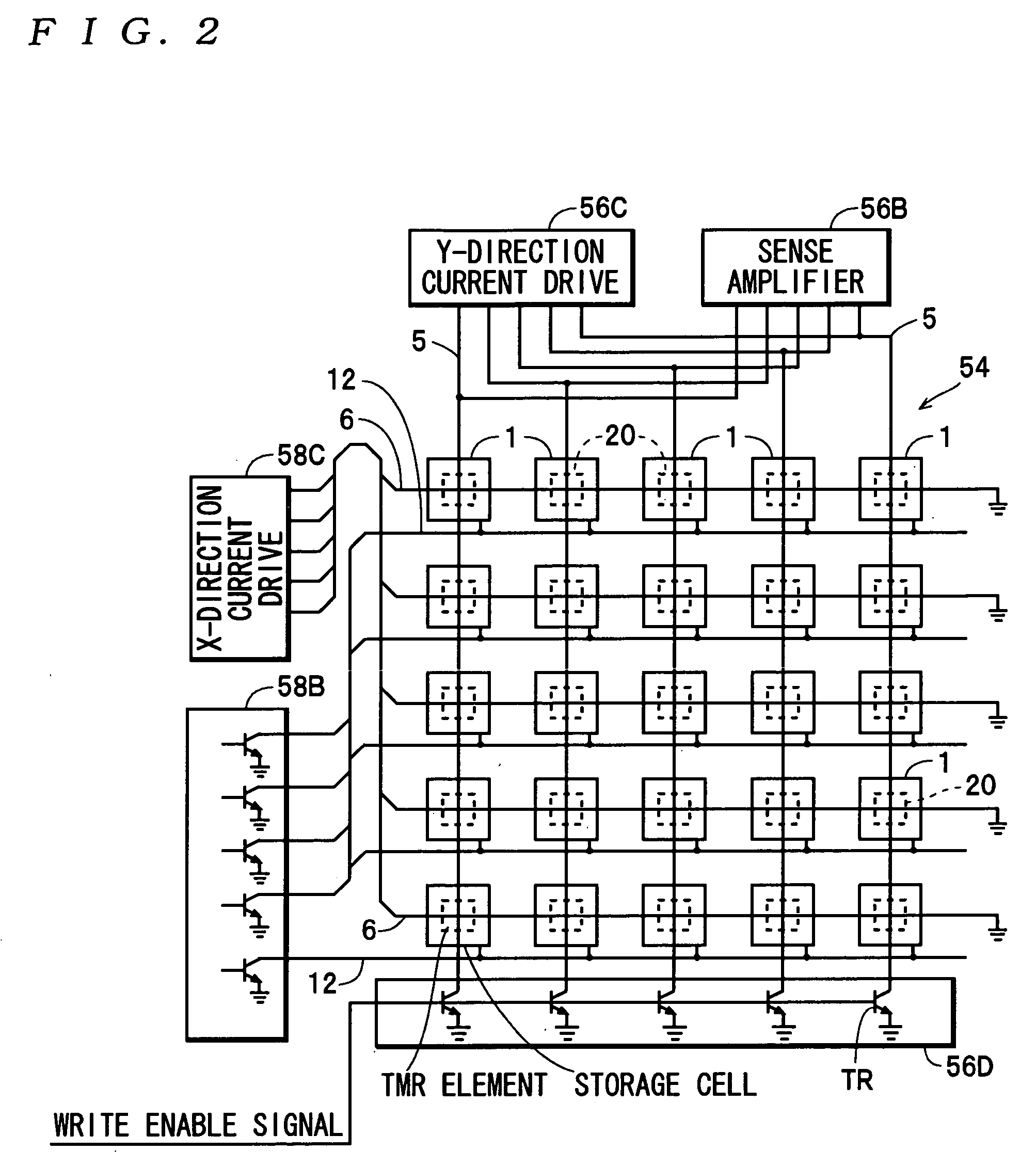
[0038] As shown in FIGS. 1 and 2, the storage cell group 54 is formed by arranging a large number of storage cells 1 at respective intersections in a matrix defined by rows in a word line direction (the X direction) and columns in a bit line direction (the Y direction). In this case, each storage cell 1 is a minimum unit for storing data, and configured to be capable of storing bit data representing “1” and “0”. More specifically, as shown in FIG. 2, each storage cell 1 is comprised of a TMR element 20, and as will be described h...
PUM
 Abstract
Description
Claims
Application Information


