Multiple level programming in a non-volatile memory device

a memory device and multi-level technology, applied in the field of memory devices, can solve the problems of program disturb condition, increase in the requirement for additional memory, and increase in the performance and complexity of electronic systems, and achieve the effect of reducing the level of program disturb

Inactive Publication Date: 2006-08-31
ROUND ROCK RES LLC
View PDF6 Cites 34 Cited by
  • Summary
  • Abstract
  • Description
  • Claims
  • Application Information

AI Technical Summary

Benefits of technology

[0008] The present invention encompasses a method for programming a multiple level memory device. The method comprises programming cells on a wordline in decreasing levels of programming voltage levels, starting with the state having the highest programming voltage. This minimizes the level of program disturb experienced by the cells on the same wordline.

Problems solved by technology

As the performance and complexity of electronic systems increase, the requirement for additional memory also increases.
One problem with MLC is that subsequent programming of additional data can cause a program disturb condition that can program bits that are not desired to be programmed.

Method used


Image

  • Multiple level programming in a non-volatile memory device
  • Multiple level programming in a non-volatile memory device
  • Multiple level programming in a non-volatile memory device

Examples


Embodiment Construction

[0017] In the following detailed description of the invention, reference is made to the accompanying drawings that form a part hereof and in which is shown, by way of illustration, specific embodiments in which the invention may be practiced. In the drawings, like numerals describe substantially similar components throughout the several views. These embodiments are described in sufficient detail to enable those skilled in the art to practice the invention. Other embodiments may be utilized and structural, logical, and electrical changes may be made without departing from the scope of the present invention. The following detailed description is, therefore, not to be taken in a limiting sense, and the scope of the present invention is defined only by the appended claims and equivalents thereof.

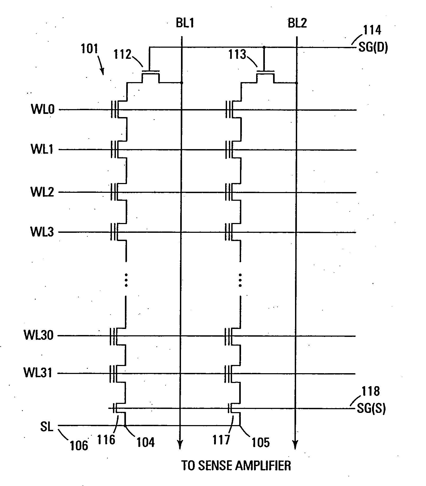
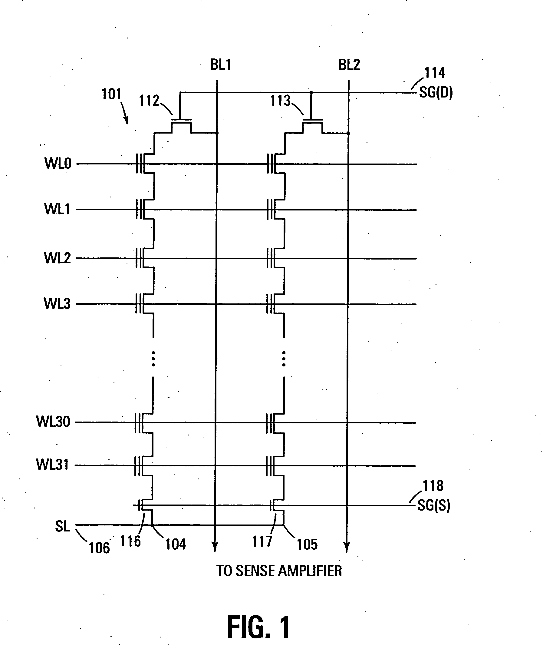
[0018]FIG. 1 illustrates a simplified diagram of one embodiment for a NAND flash memory array of the present invention. This memory is for purposes of illustration only as the present invention...


PUM


Abstract

The programming method of the present invention minimizes program disturb by initially programming cells on the same wordline with the logical state having the highest threshold voltage. The remaining cells on the wordline are programmed to their respective logical states in order of decreasing threshold voltage levels.

Description

TECHNICAL FIELD OF THE INVENTION [0001] The present invention relates generally to memory devices and in particular the present invention relates to non-volatile memory devices. BACKGROUND OF THE INVENTION [0002] Memory devices are typically provided as internal, semiconductor, integrated circuits in computers or other electronic devices. There are many different types of memory including random-access memory (RAM), read only memory (ROM), dynamic random access memory (DRAM), synchronous dynamic random access memory (SDRAM), and flash memory. [0003] Flash memory devices have developed into a popular source of non-volatile memory for a wide range of electronic applications. Flash memory devices typically use a one-transistor memory cell that allows for high memory densities, high reliability, and low power consumption. Common uses for flash memory include personal computers, personal digital assistants (PDAs), digital cameras, and cellular telephones. Program code and system data suc...

Claims


Application Information

Patent Timeline
Patent Type & Authority Applications(United States)
IPC IPC(8): G11C16/04
CPCG11C11/5628G11C16/0483G11C16/3418G11C16/3427G11C2211/5648
Inventor NAZARIAN, HAGOP A.
Owner ROUND ROCK RES LLC
Why Eureka
Try Eureka