High power single mode semiconductor laser device and fabrication method thereof

a laser device and semiconductor technology, applied in the field of semiconductor laser devices, can solve the problems of reducing the probability of high-order mode at high-power, negatively affecting the reliability of the device, and difficulty in forming the exact structure of the desired ridge, so as to achieve the effect of suppressing high-order oscillation and effective scattering of laser ligh

Inactive Publication Date: 2006-08-31
SAMSUNG ELECTRO MECHANICS CO LTD
View PDF6 Cites 49 Cited by
  • Summary
  • Abstract
  • Description
  • Claims
  • Application Information

AI Technical Summary

Benefits of technology

[0017] Preferably, the spacing of the corrugated parts is shorter than the wavelength of the laser and longer than ½ of the wavelength of the laser, in order to scatter light of the laser more effectively.
[0018] Moreover, the present invention provides a fabrication method of the semiconductor laser device including steps of: forming a first conductivity-type cladding layer, an active layer and a second conductivity-type cladding layer on a semiconductor substrate in their order; selectively etching the upper part of the second conductivity-type cladding layer, thereby forming a ridge protruding upward; and forming corrugated parts on upper surfaces of the second conductivity-type cladding layer on both sides next to the ridge for scattering light in order to suppress high order oscillation.

Problems solved by technology

A ridge semiconductor laser has small effective refractive index difference in horizontal direction, and thus there is a drawback of likely occurrence of high order mode at high power.
However, such ridge with a narrow width causes increased resistance of device or operation voltage, negatively affecting the reliability of the device, with occurrence of high order mode.
However, when forming irregular side surfaces of ridge, it may be difficult to form an exact structure of desired ridge.
Especially, when forming a ridge having a narrow width in order to realize short-wavelength single mode, it is difficult to design and form exact width due to the roughened surface of the ridge.
Moreover, when forming an upper electrode in the actual manufacturing, the area for formation of electrode may be irregular in shape due to the roughened surfaces of the ridge, which may possibly cause defective connection of the electrode, undermining the electrical characteristics of the semiconductor laser device.
Furthermore, since much heat is generated in the contact region of the ridge contacting the upper electrode, the light scattering effect of the roughened surface may be unstable due to undesired effect from the heat.

Method used


Image

  • High power single mode semiconductor laser device and fabrication method thereof
  • High power single mode semiconductor laser device and fabrication method thereof
  • High power single mode semiconductor laser device and fabrication method thereof

Examples


Embodiment Construction

[0027] Preferred embodiments of the present invention will now be described in detail with reference to the accompanying drawings.

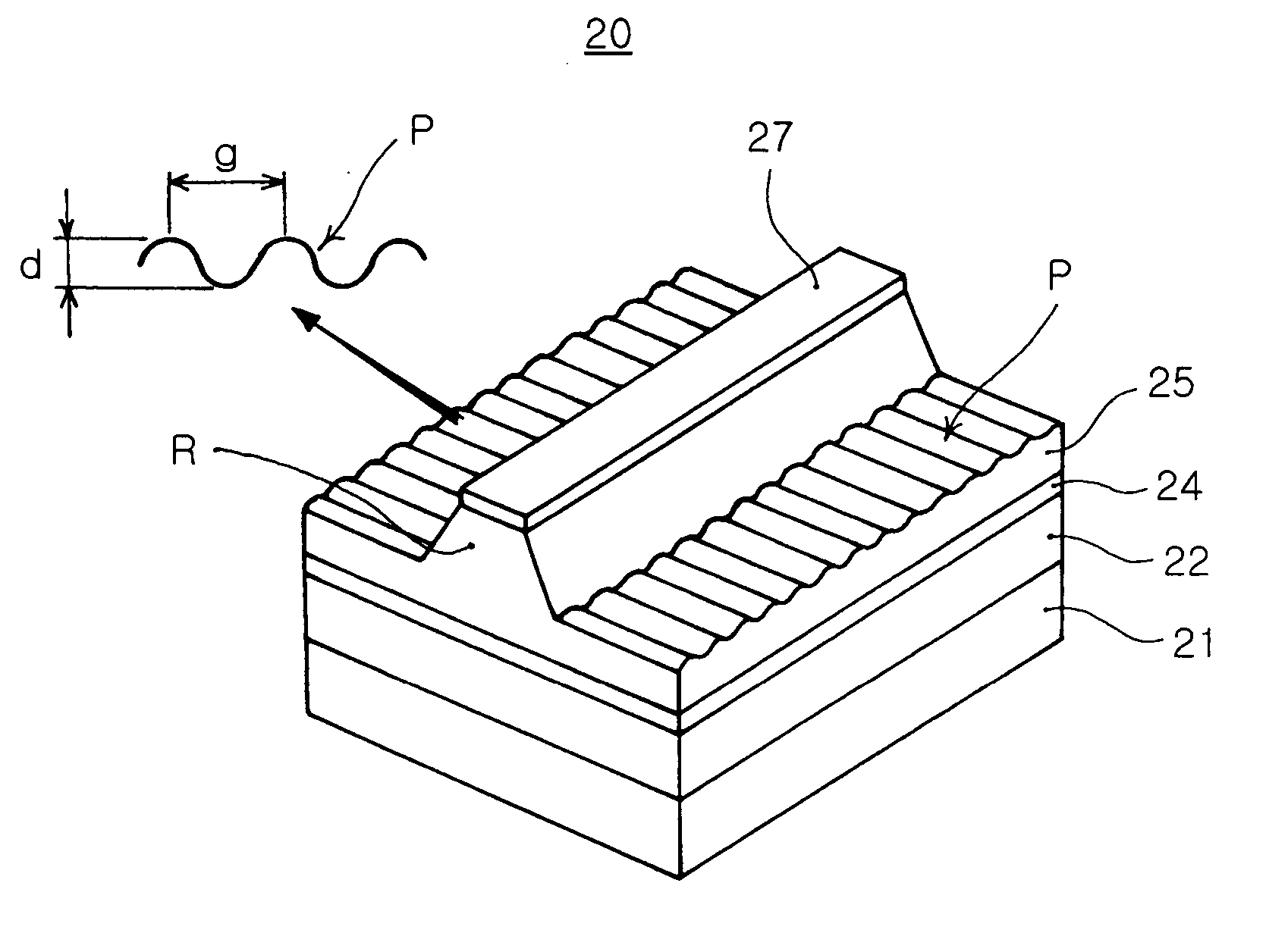
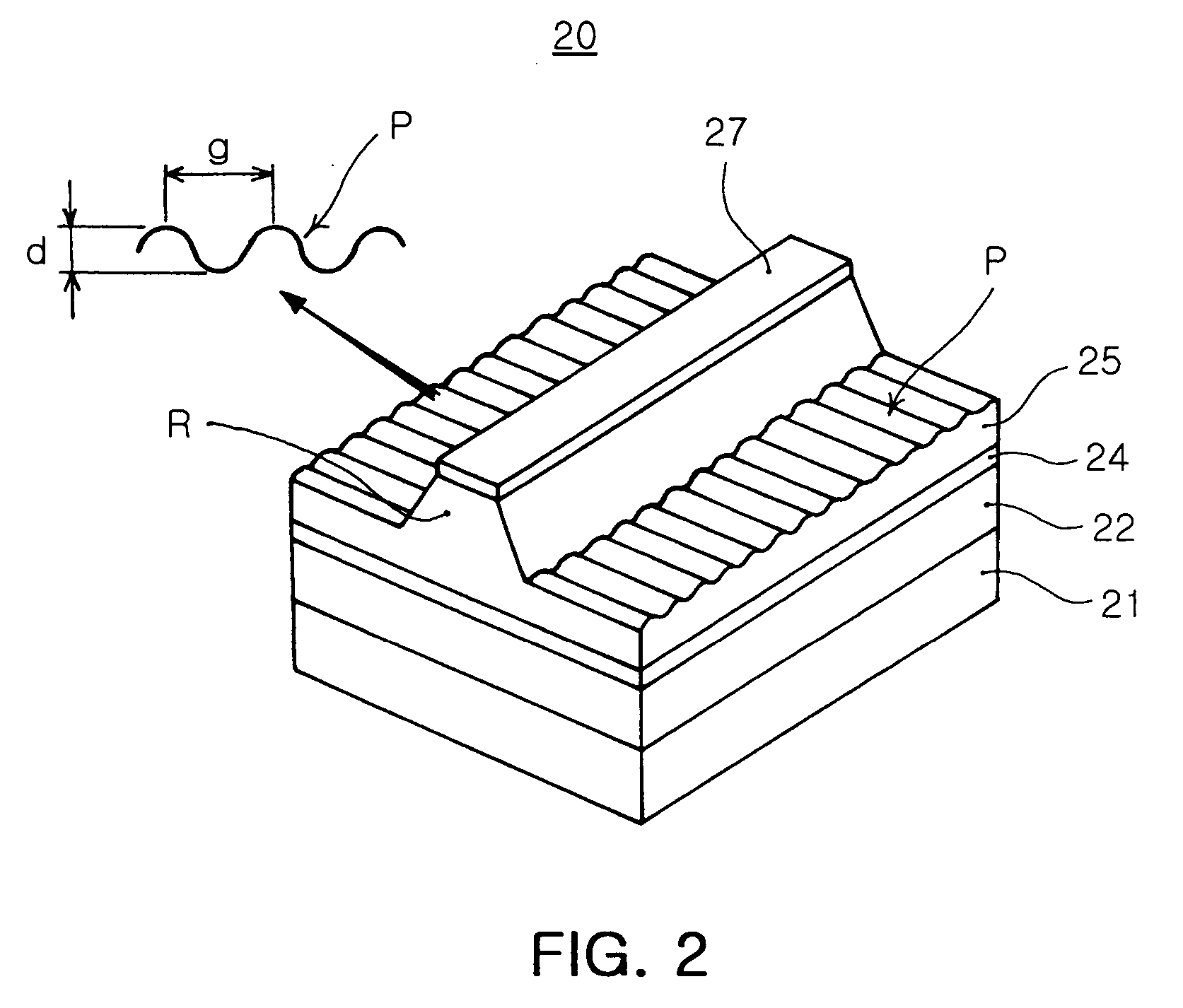
[0028]FIG. 2 is an overall perspective view illustrating a semiconductor laser device 20 according to an embodiment of the present invention. As shown in FIG. 2, the semiconductor laser device 20 includes a semiconductor substrate 21, and a first conductivity-type cladding layer 22, an active layer 24, and a second conductivity-type cladding layer 25 formed on the semiconductor substrate 21 in their order.

[0029] The upper area of the second conductivity-type cladding layer 25 is selectively etched to form a ridge R. On the top of the ridge R, a second cap layer 27 may additionally be formed.

[0030] The upper area of the second conductivity-type cladding layer 25 on both sides next to the ridge R may have wave patterns P formed for scattering light in specific regions. As in the embodiment of the present invention, the wave patterns P may have waves para...


PUM


Abstract

The present invention relates to a high-power single-mode semiconductor laser device, in which a first conductivity-type cladding layer is formed on a semiconductor substrate. An active layer is formed on the first conductivity-type cladding layer, and a second conductivity-type cladding layer is formed on the active layer, with a ridge protruding upward. The invention has corrugated parts formed on upper surfaces of the second conductivity-type cladding layer on both sides next to the ridge for scattering light in order to suppress high order mode oscillation.

Description

CLAIM OF PRIORITY [0001] This application claims the benefit of Korean Patent Application No. 2005-16780 filed on Feb. 28, 2005, in the Korean Intellectual Property Office, the disclosure of which is incorporated herein by reference. BACKGROUND OF THE INVENTION [0002] 1. Field of the Invention [0003] The present invention relates to a semiconductor laser device, and more particularly, to a semiconductor laser device capable of operating with stable single mode characteristics at high power. [0004] 2. Description of the Related Art [0005] A semiconductor laser device is capable of oscillating light having narrow frequency band (short wavelength), and has high directivity, and therefore, extensively utilized as light sources for optical pick-up devices of optical disc system and applied in variety of fields including optical communication, multiplex communication, and space communication. [0006] In general, a semiconductor laser device is manufactured as a semiconductor ridge waveguid...

Claims


Application Information

Patent Timeline
Patent Type & Authority Applications(United States)
IPC IPC(8): H01S3/098H01S5/00
CPCH01S5/0655H01S5/1028H01S5/1237H01S5/22A01F12/54A01F7/02A01F11/00
Inventor KIM, BUM JOONCHO, SOO HAENG
Owner SAMSUNG ELECTRO MECHANICS CO LTD
Why Eureka
Try Eureka