Semiconductor device and fabrication process thereof, and application thereof

a technology of semiconductor devices and semiconductors, applied in the direction of semiconductor devices, basic electric elements, electrical equipment, etc., can solve the problems of inability to reduce the concentration level of n-type regions and thermal destruction

Inactive Publication Date: 2006-09-07
RICOH KK
View PDF0 Cites 26 Cited by
  • Summary
  • Abstract
  • Description
  • Claims
  • Application Information

AI Technical Summary

Benefits of technology

[0025] In a high voltage device in which an n-channel LDMOS transistor of low ON-resistance having p-channel LDMOS transistor are integrated on the same p-type substrate, it is possible to ...

Problems solved by technology

However, in the case the concentration level of the n-type medium concentration drain region is decreased, there arises a problem that the drain region tends to cause thermal destruction with conduction of the parasitic bipolar transistor.
However, with such an approach, it was discovered that punch-through is tend to be caused between the p-type drain region...

Method used


Image

  • Semiconductor device and fabrication process thereof, and application thereof
  • Semiconductor device and fabrication process thereof, and application thereof
  • Semiconductor device and fabrication process thereof, and application thereof

Examples


Embodiment Construction

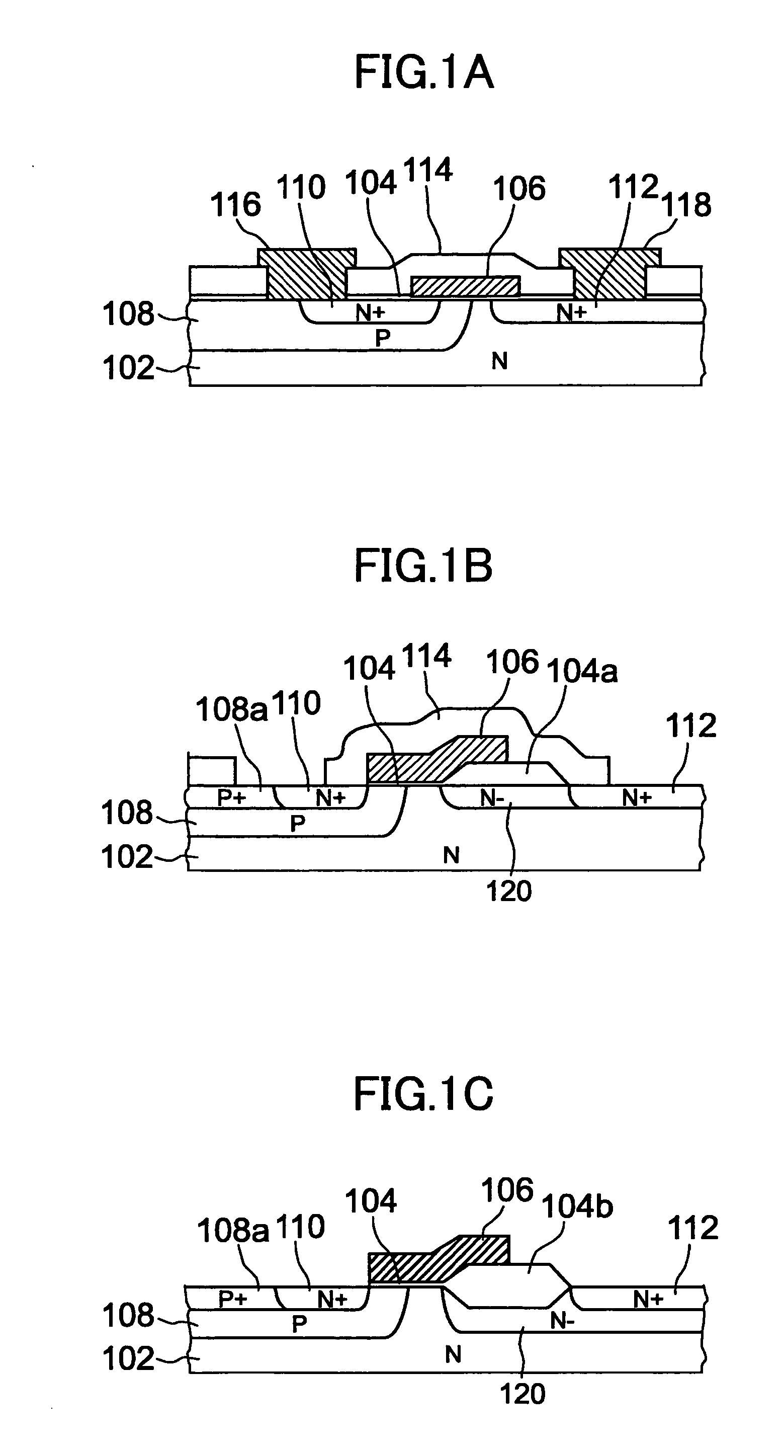
[0106] With the present specification, a “conventional MOS transistor” may any MOS transistor of conventional type including those having an LDD (lightly doped drain) region of double diffusion structure, those having a DDD (double doped drain) structure, those having an LOCOS structure having a thick oxide film at the gate edge, or the like.

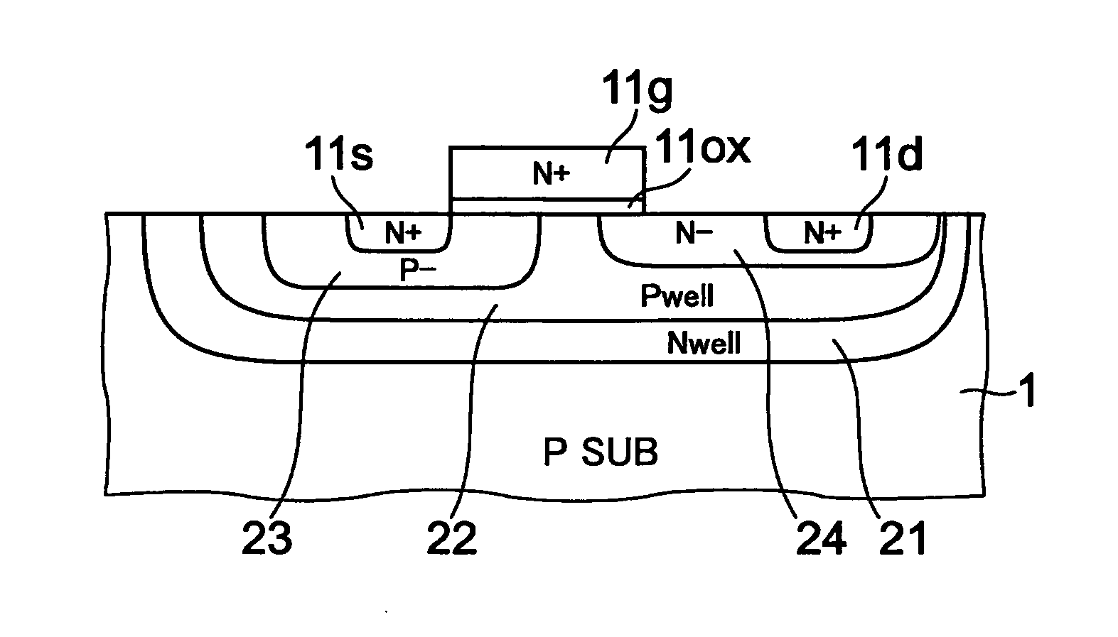
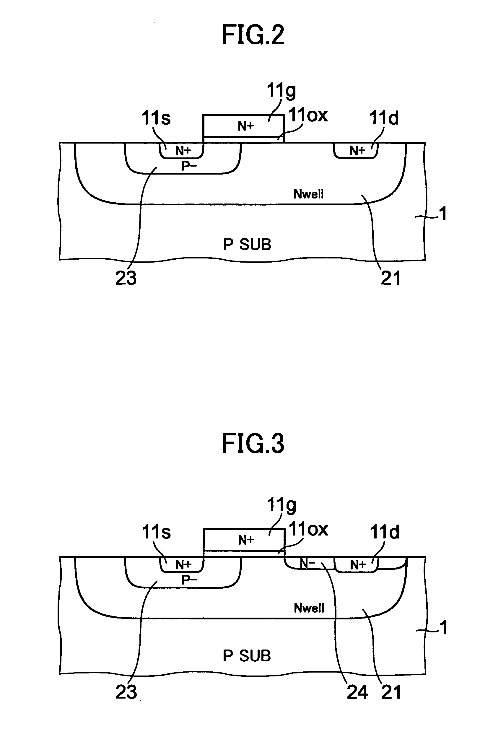
[0107]FIG. 5 is a cross-sectional view showing a semiconductor device according to an embodiment of the present invention, wherein the semiconductor device of FIG. 5 is an embodiment of the LDMOS transistor of the present invention applied to an n-channel LDMOS transistor.

[0108] Referring to FIG. 5, a drain well 21 of n-type is formed in a p-type substrate (semiconductor substrate) 1, wherein it can be seen that a p-type low-concentration well 22 is formed in the n-type drain well 21. Further, a p-type channel well 23 is formed in the p-type low-concentration well 22 such that a part of the p-type channel well 23 forms a channel region, and an...


PUM


Abstract

An LDMOS transistor includes a gate insulation film formed on a semiconductor substrate, a gate electrode formed on the gate insulation film, a drain well of a first conductivity type formed in the substrate so as to include a gate region covered with the gate electrode, a channel well of a second conductivity type formed in the drain well in a partially overlapped relationship with the gate region, a source region of the first conductivity type formed in the channel well in an overlapping manner or adjacent with a side surface of the gate electrode, a medium-concentration drain region of the first conductivity type having an intermediate concentration level and formed in the drain well at a side opposing to the source region in a manner partially overlapping with the gate region, the medium-concentration drain region being formed with a separation from the channel well, a drain region of the first conductivity type formed in the medium-concentration drain region with a separation from the gate region, a low concentration well of the second conductivity type formed inside the drain well so as to include at least a part between said channel well and the medium-concentration drain region.

Description

BACKGROUND OF THE INVENTION [0001] The present invention relates to semiconductor devices, the fabrication process thereof, and application thereof. Particularly, the present invention relates to a semiconductor device having a transistor of LDMOS structure, the fabrication process thereof, and application thereof. [0002] In this specification, an LDMOS transistor (lateral double diffuse insulation gate field transistor) is defined as a field effect transistor having a low impurity concentration layer formed so as to surround the source region with a conductivity type opposite to the conductivity type of the source or drain region. The LDMOS transistor thereby uses a surface part of the low impurity concentration layer right underneath the gate electrode as a channel region. Further, “conventional MOS transistor” used in this specification is defined as a MOS transistor having the structure in which a drain region is formed with an impurity concentration level higher than in a chann...

Claims


Application Information

Patent Timeline
IPC IPC(8): H01L29/76H01L21/336
CPCH01L21/823814H01L21/823857H01L21/823892H01L27/0922H01L27/0928H01L29/1045H01L29/1083H01L29/7816H01L29/7835
Inventor FUJIMOTO, KEIJI
Owner RICOH KK
Why Eureka
Try Eureka