Electrically conductive line, method of forming an electrically conductive line, and method of reducing titanium silicide agglomeration in fabrication of titanium silicide over polysilicon transistor gate lines

a technology of polysilicon transistor and electrode, which is applied in the direction of electrical equipment, semiconductor devices, semiconductor/solid-state device details, etc., can solve the problems of titanium silicide relative to the underlying polysilicon, fatal short, and inability to predict or control the degree of agglomeration, so as to reduce the agglomeration of titanium silicid

Active Publication Date: 2006-09-07
MICRON TECH INC
View PDF95 Cites 14 Cited by
  • Summary
  • Abstract
  • Description
  • Claims
  • Application Information

AI Technical Summary

Problems solved by technology

One problem associated with the fabrication of such lines is known as agglomeration of the titanium silicide relative to the underlying polysilicon.
For transistor gate lines, the migration can even be to completely through the gate dielectric, thereby causing a fatal short.
Further, the degree of agglomeration is not predictable or controllable from device to device.
For transistor gates that are not fatally shorted, this undesirably creates different operating characteristics for different devices.

Method used


Image

  • Electrically conductive line, method of forming an electrically conductive line, and method of reducing titanium silicide agglomeration in fabrication of titanium silicide over polysilicon transistor gate lines
  • Electrically conductive line, method of forming an electrically conductive line, and method of reducing titanium silicide agglomeration in fabrication of titanium silicide over polysilicon transistor gate lines
  • Electrically conductive line, method of forming an electrically conductive line, and method of reducing titanium silicide agglomeration in fabrication of titanium silicide over polysilicon transistor gate lines

Examples


Embodiment Construction

[0025] This disclosure of the invention is submitted in furtherance of the constitutional purposes of the U.S. Patent Laws “to promote the progress of science and useful arts” (Article 1, Section 8).

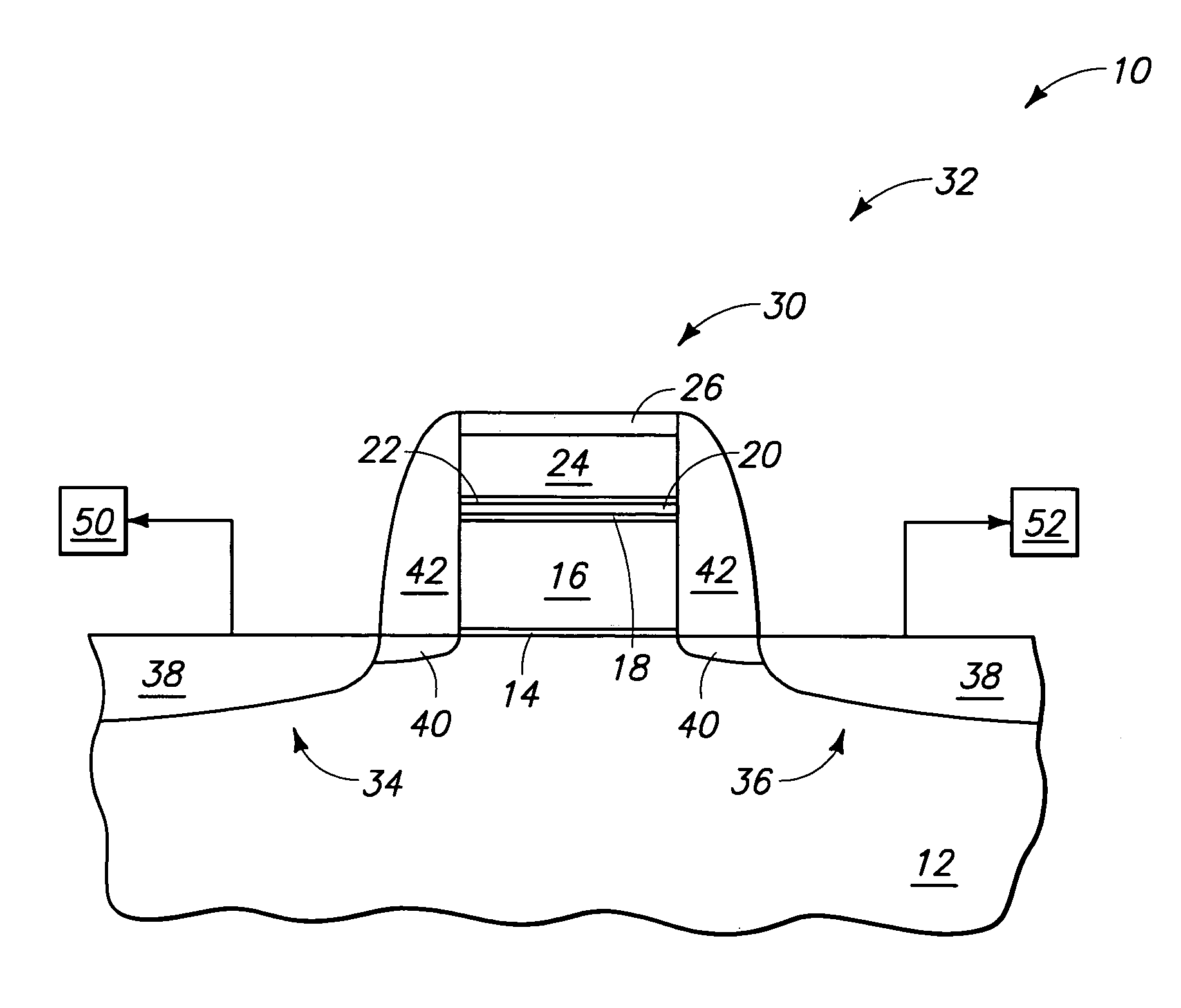
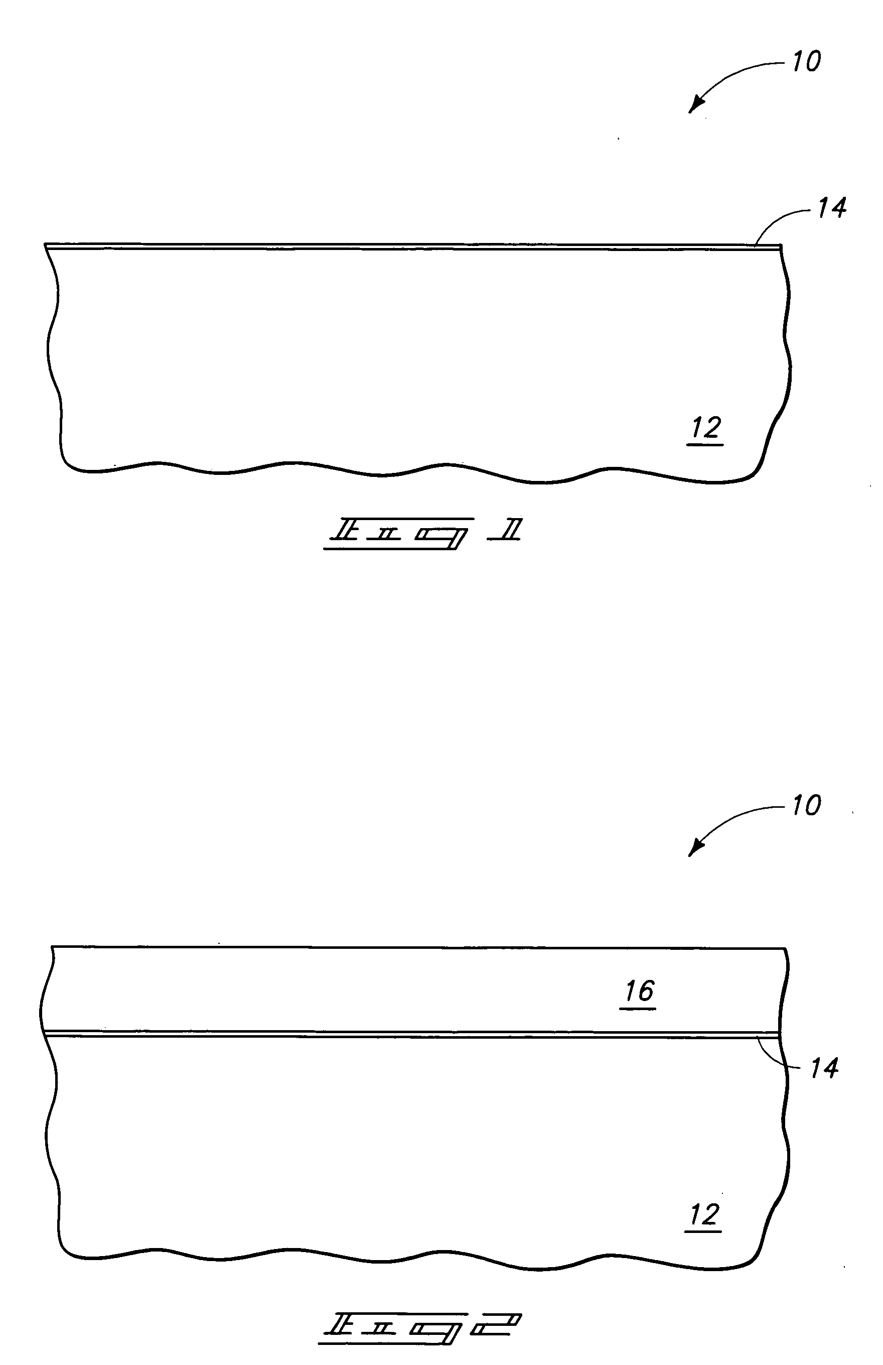
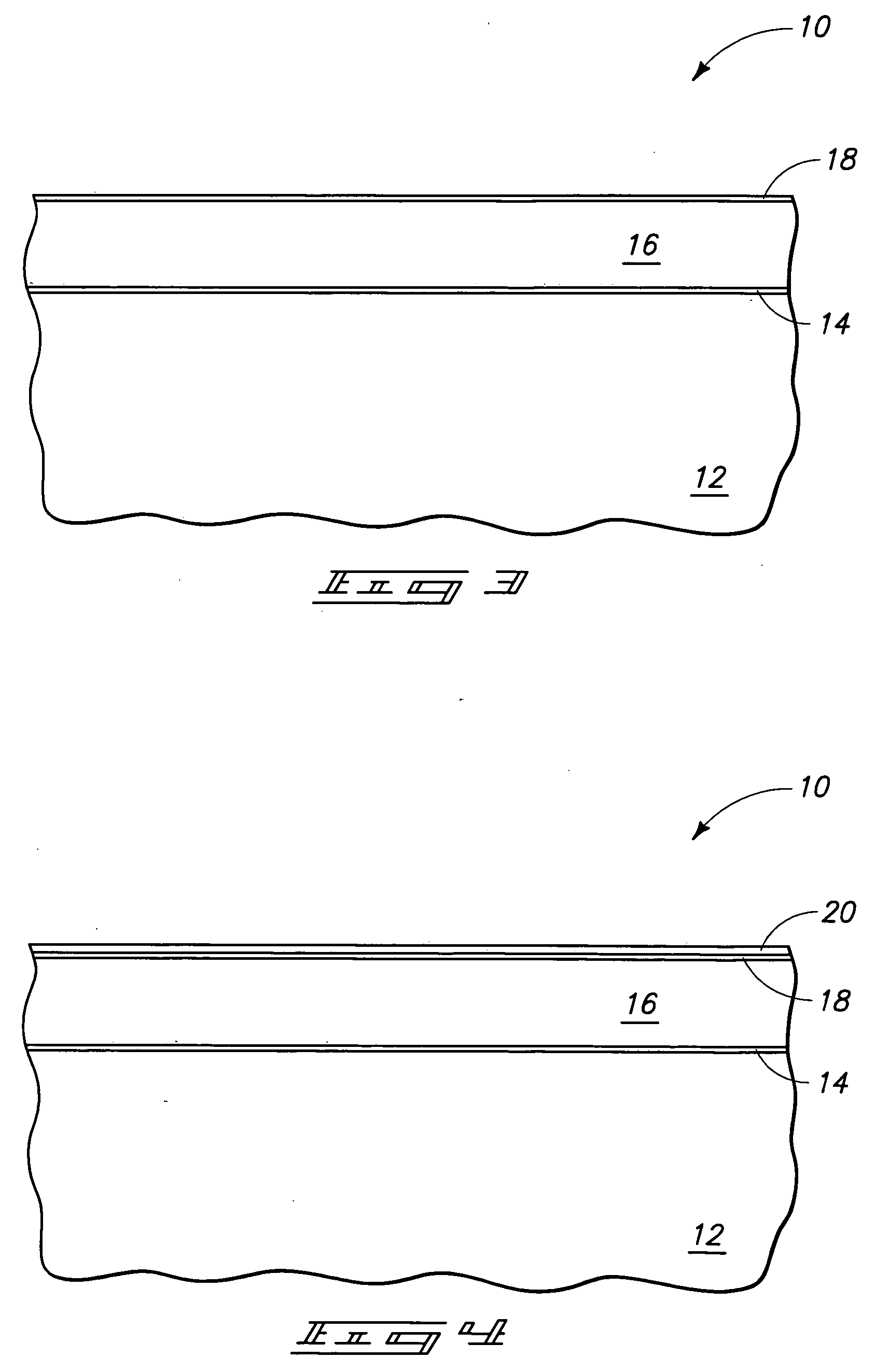
[0026] A preferred method of forming an electrically conductive line, and particularly a field effect transistor gate line, is initially described with reference to FIGS. 1-9. Referring to FIG. 1, a substrate fragment is indicated generally with the reference numeral 10. Such preferably comprises a semiconductor substrate, for example as substrate comprising a bulk monocrystalline silicon region 12 having a gate dielectric layer 14 formed thereover. In the context of this document, the term “semiconductor substrate” or “semiconductive substrate” is defined to mean any construction comprising semiconductive material, including, but not limited to, bulk semiconductive materials such as a semiconductive wafer (either alone or in assemblies comprising other materials thereon), and semicondu...


PUM

PropertyMeasurementUnit
thicknessesaaaaaaaaaa
thicknessaaaaaaaaaa
thicknessaaaaaaaaaa

Abstract

The invention includes an electrically conductive line, methods of forming electrically conductive lines, and methods of reducing titanium silicide agglomeration in the fabrication of titanium silicide over polysilicon transistor gate lines. In one implementation, a method of forming an electrically conductive line includes providing a silicon-comprising layer over a substrate. An electrically conductive layer is formed over the silicon-comprising layer. An MSixNy-comprising layer is formed over the electrically conductive layer, where “x” is from 0 to 3.0, “y” is from 0.5 to 10, and “M” is at least one of Ta, Hf, Mo, and W. An MSiz-comprising layer is formed over the MSixNy-comprising layer, where “z” is from 1 to 3.0. A TiSia-comprising layer is formed over the MSiz-comprising layer, where “a” is from 1 to 3.0. The silicon-comprising layer, the electrically conductive layer, the MSixNy-comprising layer, the MSiz-comprising layer, and the TiSia-comprising layer are patterned into a stack comprising an electrically conductive line. Other aspects and implementations are contemplated.

Description

TECHNICAL FIELD [0001] This invention relates to electrically conductive lines, to methods of forming electrically conductive lines, and to methods of reducing titanium silicide agglomeration in the fabrication of titanium silicide over polysilicon transistor gate lines. BACKGROUND OF THE INVENTION [0002] One common component found in integrated circuits is an electrically conductive line. Such might form part of a device or subcircuit, or interconnect various devices. One common conductive line is a transistor gate of a field effect transistor device. Such are commonly used in memory integrated circuitry, for example dynamic random access memory (DRAM) circuitry. Individual memory cells of DRAM circuitry include a field effect transistor having one source / drain region thereof electrically connected with a storage capacitor, and the other source / drain region electrically connected with a bitline. The conductive transistor gate lines are commonly referred to as wordlines, with indivi...

Claims


Application Information

Patent Timeline
Patent Type & Authority Applications(United States)
IPC IPC(8): H01L23/52H01L21/44H01L21/8234H01L29/772
CPCH01L21/28061H01L21/2855H01L21/76838H01L27/10891H01L2221/1078H01L2924/0002H10B12/488H01L2924/00H01L23/485H01L29/4933H01L21/28518
Inventor PAN, QILI, JIUTAOHU, YONGJUN JEFFMCTEER, ALLEN
Owner MICRON TECH INC
Why Eureka
Try Eureka