
Feedback control circuit

a control circuit and feedback technology, applied in the field of feedback control circuits, can solve the problems of changing the state of the system, external components such as capacitors attached to the integrator or low-pass filter, being subjected to the noise of the circuit, etc., and achieve the effect of reducing the influence of disturban

Active Publication Date: 2006-09-07
ASAHI KASEI ELECTRONICS CO LTD
View PDF1 Cites 2 Cited by
  • Summary
  • Abstract
  • Description
  • Claims
  • Application Information

AI Technical Summary

Benefits of technology

[0012] According to the present invention, the feedback control circuit includes first inverting means for inverting a polarity of the differential signal when the output of the filter means becomes a predetermined value; second inverting means installed at a post-stage of the filter means, for inverting an output polarity of a signal based on the output signal of the filter means when the first inverting means inverts the polarity of the differential signal; and add-subtract means for generating, when the first inverting means inverts the polarity of the differential signal, the control value by adding to or subtracting from the signal inverted by the second inverting means a value of that signal at inversion, or a specified value. Therefore it can reduce the influences of the disturbance, which is added to the integrating circuit or high frequency eliminating circuit, on the output to a fraction of the conventional system with using the same voltage range as the output range of the integrating circuit or high frequency eliminating circuit.

Problems solved by technology

Although the AGC or PLL uses an integrator or low-pass filter in the feedback control circuit, the output of the integrator or low-pass filter is limited within the power supply voltage of the circuit.
Increasing the gain, however, presents a problem of greatly changing the state of the system because of noise added to the output of the integrating circuit or low-pass filter.
In addition, the integrator or low-pass filter includes a high impedance node, which is sensitive to noise.
In addition, an external component such as a capacitor attached to the integrator or low-pass filter is subjected to circulate noise on a board.
Even if all the components are integrated into an IC, the circulate noise from a substrate cannot be eliminated completely, and hence the integrator or low-pass filter is subjected to influences of the noise.

Method used


Image

  • Feedback control circuit
  • Feedback control circuit
  • Feedback control circuit

Examples


embodiment 1

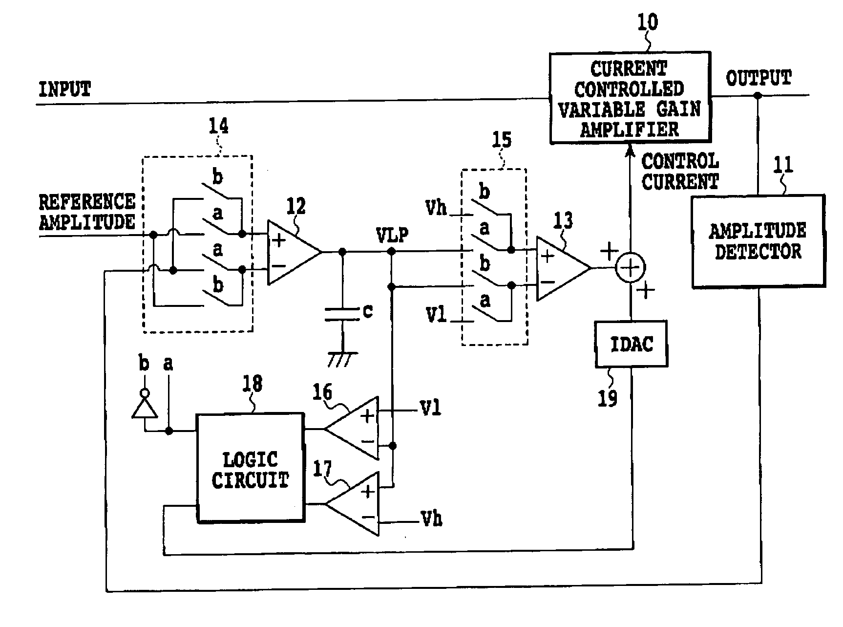
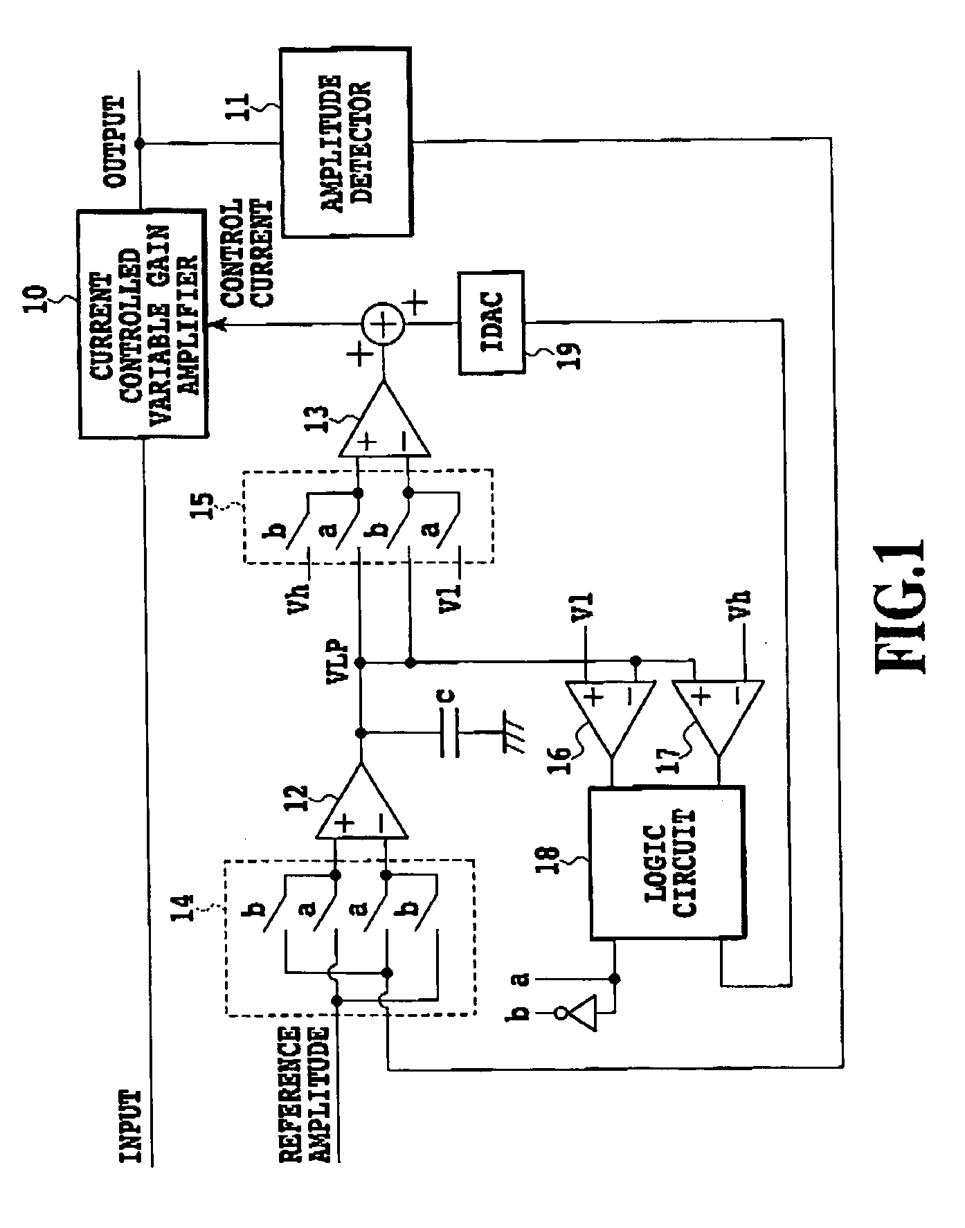
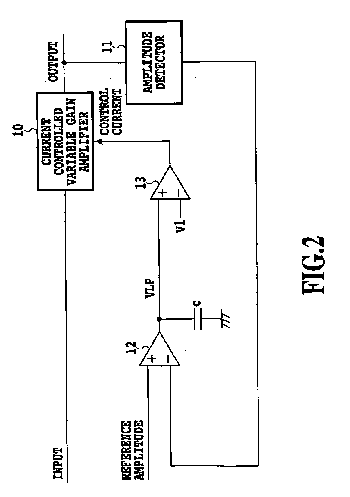
[0025]FIG. 1 is a block diagram showing a configuration of an embodiment of a feedback control circuit in accordance with the present invention. FIG. 2 is a block diagram showing a basic configuration of the embodiment 1 as shown in FIG. 1. The feedback control circuit has a function that maintains its output amplitude at a target level even if the input signal amplitude varies.

[0026] In FIGS. 1 and 2, the reference numeral 10 designates a current controlled variable gain amplifier; 11 designates an amplitude detector; reference numerals 12 and 13 each designate a current output type differential amplifier; 14 and 15 each designate an input switching unit; 16 and 17 each designate a comparator; the reference numeral 18 designates a logic circuit; and 19 designates an IDAC (current output type DA converter).

[0027] First, a basic configuration of the embodiment 1 shown in FIG. 2 will be described.

[0028] The input signal is input to the variable gain amplifier 10, the gain of which i...

embodiment 2

[0044] First, the basic configuration of the embodiment 2 as shown in FIG. 5 will be described.

[0045] The PFC 22 compares the phase of an input clock CLK with the phase of a clock NCKO obtained by dividing the output CKO of the CCO by N by the frequency divider 26. When the CLK leads the NCKO in the phase, the PFC 22 sets the UP output at the “H” level for an interval corresponding to the phase difference, and when the CLK lags behind the NCKO in the phase, the PFC 22 sets the DN output at the “H” level for an interval corresponding to the phase difference. The CP 23 outputs a current Icp when UP is at the “H” level and a current −Icp when DN is at the “H” level, and outputs zero when both the UP and DN are at the “H” level or at the “L” level.

[0046] The loop filter 24, which consists of a capacitor C and a resistor R, integrates the phase comparing result by storing the charge, that is, the current output for the time corresponding to the phase difference, into the capacitor C. Th...


PUM


Abstract

The output amplitude of a variable gain amplifier is compared with a reference value by a differential amplifier. When the amplitude is less than the reference value, the gain of the variable gain amplifier is increased to augment the output amplitude. When the amplitude is greater than the reference value, the gain of the variable gain amplifier is decreased to reduce the output amplitude. Only part of the variable gain range of the variable gain amplifier is corresponded to the potential at VLP by installing an input switching unit for inverting the output polarity of the differential amplifier, an input switching unit for inverting the output polarity of a differential amplifier, comparator, an IDAC, and a logic circuit for controlling the ON and OFF of switches of the input switching units and the output current value of the IDAC.

Description

BACKGROUND OF THE INVENTION [0001] 1. Field of the Invention [0002] The present invention relates to a feedback control circuit, and more particularly to a feedback control circuit using an integrating circuit or a high frequency eliminating circuit. [0003] 2. Description of Related Art [0004] Generally, the control that compares an output with a reference value and minimizes the difference between the two is know as PID (proportional-plus-integral-plus-derivative) control in the automatic control (for example, see, Shigeru Kurosu, “Introduction to Control Engineering” pp. 77-86, 2nd edition, POWERSHA Inc. May 30, 1994). In the field of electric circuits, the PID control is applied, for example, to AGC (Automatic Gain Control) (see, Green, D. “Global stability analysis of automatic gain control circuits” Circuits and Systems, IEEE Transactions on, Volume 30, Issue 2, February 1983, pp. 78-83, for example), or to a PLL (Phase-Locked Loop) (see, Larsson, P. “Measurements and analysis ...

Claims


Application Information

Patent Timeline
Patent Type & Authority Applications(United States)
IPC IPC(8): H03L7/00
CPCH03G3/3036H03L7/0891H03L7/093H03L7/18
Inventor KONNO, YOSHIAKI
Owner ASAHI KASEI ELECTRONICS CO LTD
Learn More