System and method for optimizing interconnections of components in a multichip memory module

a multi-chip memory module and interconnection optimization technology, applied in computing, instruments, data conversion, etc., can solve the problems of consuming more space, skewing can seriously limit the operating speed of memory devices, and efforts are often frustrated

Active Publication Date: 2006-09-07
MICRON TECH INC
View PDF59 Cites 53 Cited by
  • Summary
  • Abstract
  • Description
  • Claims
  • Application Information

AI Technical Summary

Problems solved by technology

These efforts are often frustrated by cross talk and skew of signals being communicated on and to the memory modules, particularly as the memory modules become smaller.
Overall, the necessity of such careful considerations in both distancing conductors from each other and in creating equivalent path lengths to minimize the effects of cross talk and skew complicates efforts to produce effective memory modules with small dimensions.
This potential for signal skew can seriously limit the operating speed of the memory devices 102-116.
This consumes more space, increases propagation delay, and may adversely affect signal integrity.
If each memory module has a layout like the DIMMs 100a, 100b of FIG. 1, layout and routing congestion problems arise.
This skew presents timing problems for the memory hub, particularly with regard to read data from the DRAMs which will arrive at the hub at different times yet must be accurately captured.
The hub could execute a synchronization process for each DRAM, but this would increase the complexity and cost of the memory hub.
Routing congestion problems also arise with this layout due to all the signals that must be routed between the devices and the hub.
While more layers could be added to the circuit board 140, this increases the complexity and cost of the board.

Method used


Image

  • System and method for optimizing interconnections of components in a multichip memory module
  • System and method for optimizing interconnections of components in a multichip memory module
  • System and method for optimizing interconnections of components in a multichip memory module

Examples


Embodiment Construction

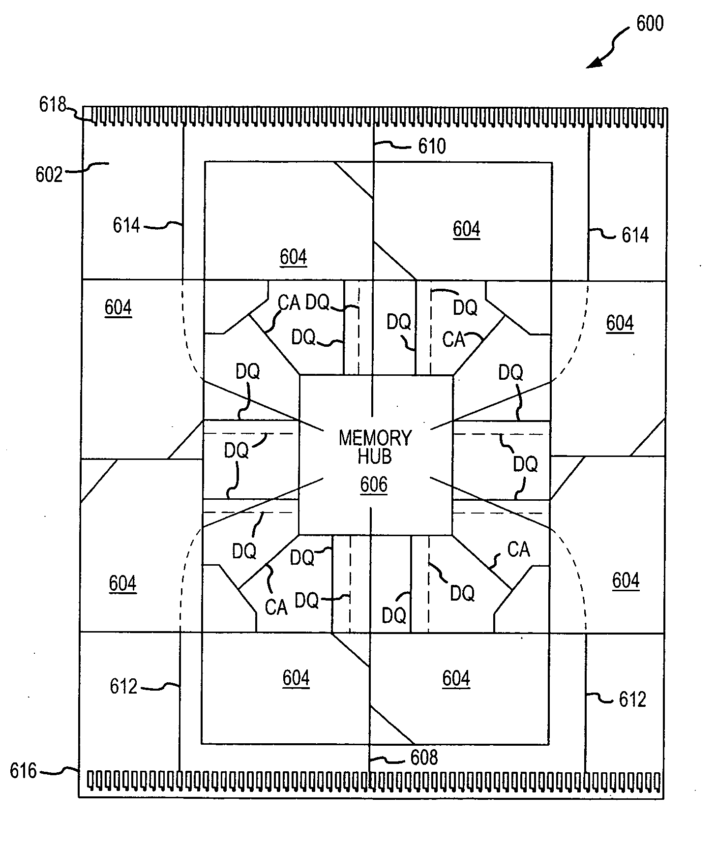
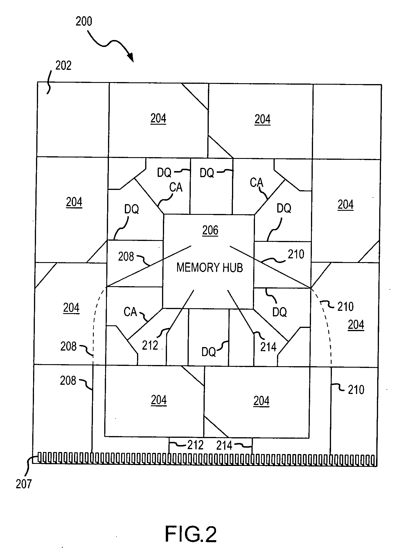
[0022]FIG. 2 is a schematic top view of a memory module 200 including a circuit board 202 on which eight memory devices 204 are physically positioned around a memory hub 206 and are physically oriented to minimize the skew of signals among the memory devices according to one embodiment of the present invention. The position and orientation of each memory device 204 is such that the electrical characteristics of conductive lines or busses interconnecting the memory device and the memory hub 206 are substantially the same for all memory devices, minimizing the skew of signals among the memory devices and thereby allowing for high-speed operation of the memory module as will be described in more detail below. In the following description, certain details are set forth to provide a sufficient understanding of the present invention. One skilled in the art will understand, however, that the present invention may be practiced without these particular details.

[0023] The construction of the...


PUM


Abstract

An apparatus and method couples memory devices in a memory module to a memory hub on the module such that signals traveling from the hub to the devices have approximately the same propagation time regardless of which device is involved. Specifically, the devices are arranged around the hub in pairs, with each pair of devices being oriented such that a functional group of signals for each device in the pair, such as the data bus signals, are positioned adjacent each other on a circuit board of the module. This allows for a data and control-address busses having approximately the same electrical characteristics to be routed between the hub and each of the devices. This physical arrangement of devices allows high speed operation of the module. In one example, the hub is located in the center of the module and eight devices, four pairs, are positioned around the hub.

Description

TECHNICAL FIELD [0001] The present invention relates generally to computer memory modules, and, more specifically, to methods and apparatus for improving signal integrity between a memory hub or other component on a memory module and memory devices contained on the memory module. BACKGROUND OF THE INVENTION [0002] A main focus of the contemporary semiconductor industry is the creation of smaller, faster, higher density, and more efficient memory modules. These efforts are often frustrated by cross talk and skew of signals being communicated on and to the memory modules, particularly as the memory modules become smaller. Cross talk is an inductive effect which can arise when a variable current flows through a conductor. Variable current creates a corresponding variable magnetic field surrounding the conductor capable of inducing a disruptive signal in any adjacent conductors passing through the magnetic field. As a consequence, the placement of conductors in a memory module must be c...

Claims


Application Information

Patent Timeline
Patent Type & Authority Applications(United States)
IPC IPC(8): G06F3/00G06F13/00G06F12/00G06F13/16G11C5/00
CPCG06F13/1684G11C5/025G11C5/04
Inventor JANZEN, JEFFERY W.
Owner MICRON TECH INC
Why Eureka
Try Eureka