
Single-cycle low-power CPU architecture

Inactive Publication Date: 2006-09-07
ATMEL CORP
View PDF9 Cites 7 Cited by
  • Summary
  • Abstract
  • Description
  • Claims
  • Application Information

AI Technical Summary

Benefits of technology

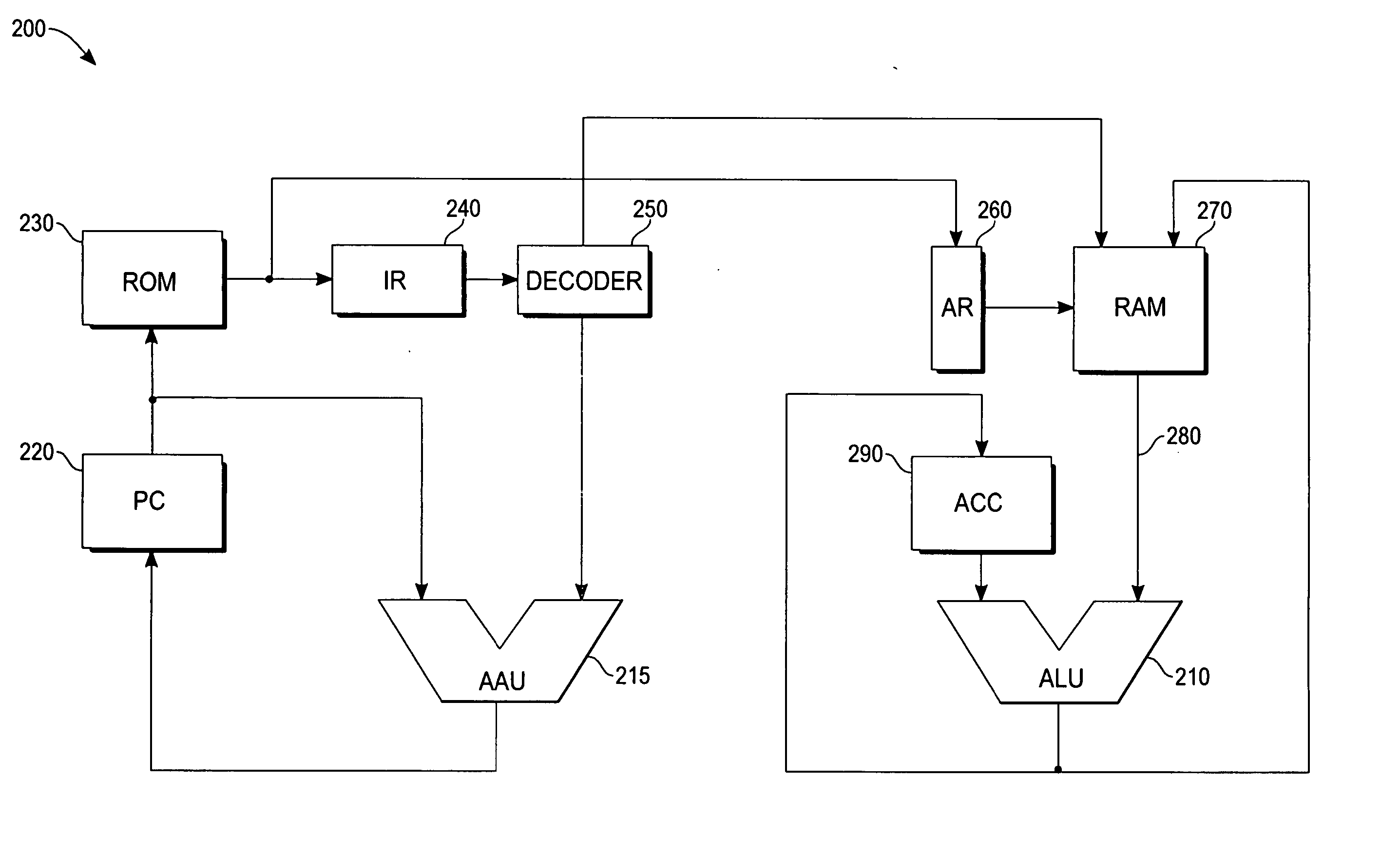
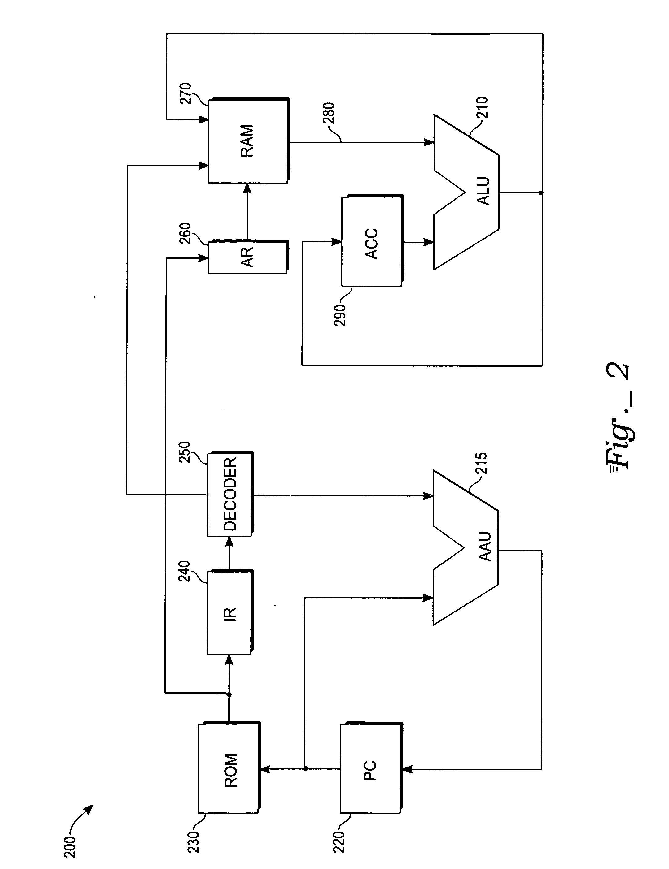
[0010] A further improvement over the prior art is implemented by utilizing separate registers to provide random access memory (RAM) read address storage and write address storage. The dedicated RAM write address register makes it possible to defer a write operation associated with an instruction. The deferred write operation enables instructions to effectively complete operation during a given system clock cycle, with the associated write operation occurring in the following system clock cycle. The deferred RAM write capability makes it possible to avoid stalling the instruction pipeline by a pending write operation. The separate RAM read address storage and RAM write address storage registers also enable a data pass-through capability in the RAM: When both registers are provided with the same RAM address, data present in a RAM data storage register is immediately made available on the RAM output, while simultaneously being written to the addressed storage area. The pass-through feature makes it possible for the results of a computation to be available to further processing with minimum time delay, further enabling the capabilities of the instruction pipeline.
[0011] An instruction pre-decode path is provided from the read-only memory (ROM) to the random access memory (RAM) which is used to speed execution of register operations, bypassing the normal decode process. In addition a register bank forwarding path prevents the pipeline from stalling when a register operation follows a change of the active register bank in a program status word (PSW).
[0013] The combined improvements embodied by the dedicated data paths, the instruction pre-decode and bank forwarding, and the separate RAM read and write address registers allows a complete a register increment instruction in a single system clock cycle, and a register indirect increment in two system clock cycles.

Problems solved by technology

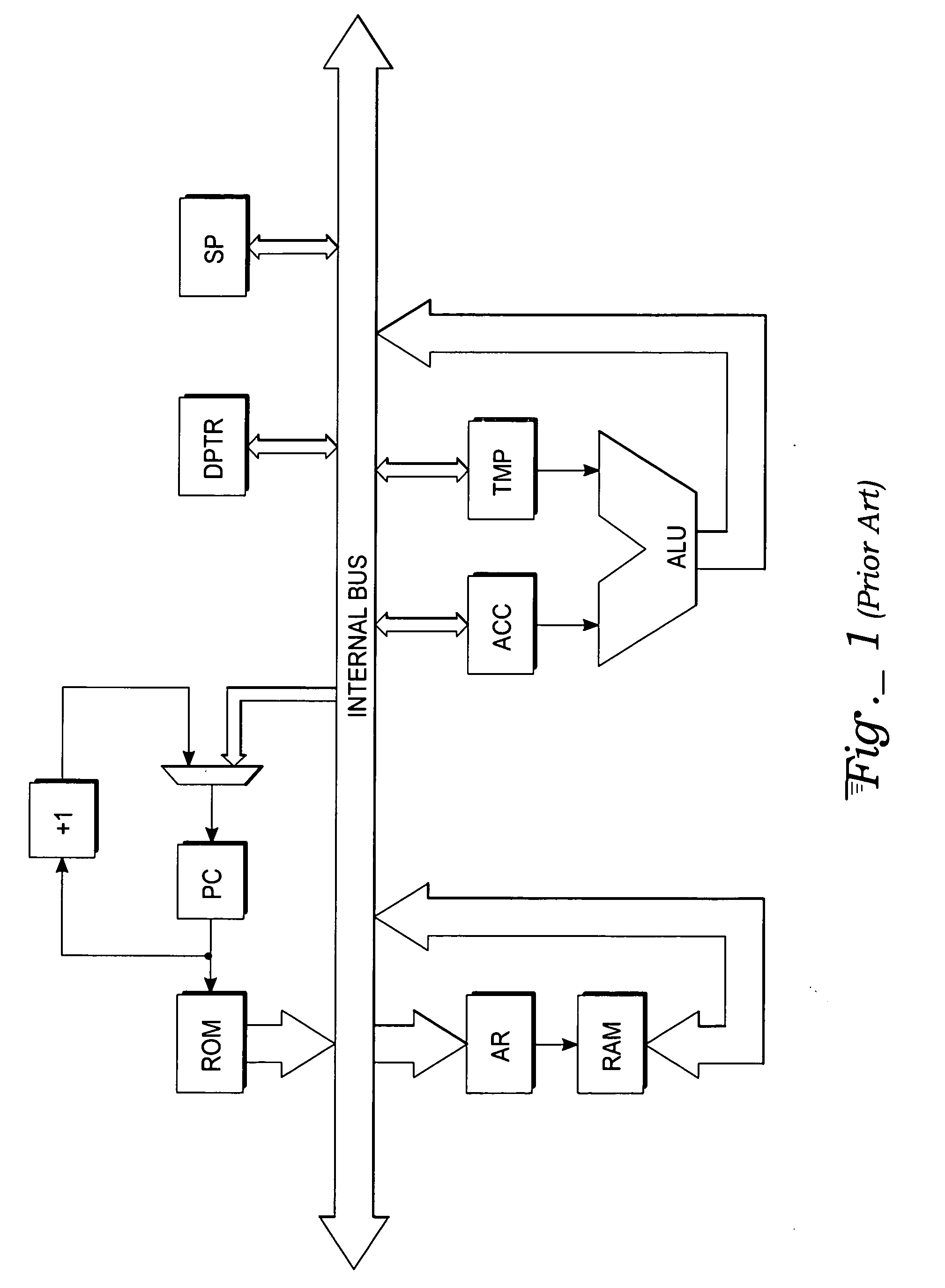
Established designs are usually optimized in terms of minimizing the gate count needed to realize the required logic, and typically offer little opportunity for improvement.

Method used


Image

  • Single-cycle low-power CPU architecture
  • Single-cycle low-power CPU architecture
  • Single-cycle low-power CPU architecture

Examples


Embodiment Construction

[0026] With reference to FIG. 2, a central processing unit (CPU) pipeline architecture portion 200 according to an exemplary embodiment of the present invention comprises an arithmetic logic unit (ALU) 210 having a first data input, a second data input, and a data output. In the exemplary embodiment, the arithmetic logic unit (ALU) 210 is configured to operate upon eight-bit binary numbers. The data output of the arithmetic logic unit (ALU) 210 is coupled to an accumulator register (ACC) 290, and to a random access memory (RAM) 270. In addition the exemplary embodiment contains an address arithmetic unit (AAU) 215 having a first data input, a second data input, and a data output. In the exemplary embodiment, the address arithmetic unit (AAU) 215 is configured to operate upon sixteen-bit binary numbers. The data output of the address arithmetic unit (AAU) 215 is coupled to a program counter (PC) 220.

[0027] The random access memory (RAM) 270 is organized as 256×8 bits, for a total st...


PUM


Abstract

An n architecture for implementing an instruction pipeline within a CPU comprises an arithmetic logic unit (ALU), an address arithmetic unit (AAU), a program counter (PC), a read-only memory (ROM) coupled to the program counter, to an instruction register, and to an instruction decoder coupled to the arithmetic logic unit. A random access memory (RAM) is coupled to the instruction decoder, to the arithmetic logic unit, and to a RAM address register.

Description

RELATED ART [0001] This application incorporates by reference, in its entirety, all material found in co-pending provisional application, Ser. No. ______, filed Mar. 4, 2005, and having the same inventive entity.TECHNICAL FIELD [0002] The present invention is related to integrated circuits. More specifically, the present invention is an apparatus and method for a microcontroller architecture which implements an instruction pipeline to speed program execution and reduce power consumption. BACKGROUND ART [0003] Raising the system clock frequency is an often-used method for improving the computational performance of a central processing unit (CPU) within a microprocessor or microcontroller. It is appreciated by those skilled in the art that the typical power (P) consumed by a CPU depends upon the total CPU gate capacitance (C), the power supply voltage (V), and the system clock frequency (f) according to the formula: P∝CV2f [0004] The power consumption can be reduced by lowering C, V, ...

Claims


Application Information

Patent Timeline
IPC IPC(8): G06F9/44
CPCG06F9/30098G06F9/3012G06F9/382G06F9/3824G06F9/3826
Inventor FROEMMING, BENJAMIN F.LAMBRACHE, EMIL
Owner ATMEL CORP
Learn More