
Semiconductor integrated circuit device, and apparatus and program for designing same

a technology of integrated circuit device and semiconductor, applied in the direction of semiconductor device, semiconductor/solid-state device details, electrical apparatus, etc., can solve the problems of increased labor and burden, inability of cells to function normally, and inability to design and verify

Active Publication Date: 2006-09-14
RENESAS ELECTRONICS CORP
View PDF16 Cites 97 Cited by
  • Summary
  • Abstract
  • Description
  • Claims
  • Application Information

AI Technical Summary

Benefits of technology

[0007] The inventor has independently discovered an entirely new design method, apparatus and semiconductor device that utilize cell library resources effectively to make it possible to convert a cell for which the well potential is the power-supply potential to a cell that supplies any well potential.
[0033] In accordance with the present invention, an existing cell having taps for supplying a power-supply potential and ground potential as well potentials is converted, whereby the cell can be replaced by a cell for supplying any potentials as the well potentials and effective utilization of cell library resources is made possible.
[0034] Further, according to the present invention, the burden involved in cell design can be suppressed by automatically making a conversion to a cell that supplies any potential as well potential.
[0035] Further, according to the present invention, an increase in chip area can be suppressed by placing an interconnect that supplies power-supply potential and a diffusion region that is connected to this interconnect by a contact at positions where they will overlap each other.

Problems solved by technology

Consequently, if it is attempted to alleviate new design load through a method of providing a layout that eliminates the tap within the cell and supplies any well potential separately, a cell having a batting connection is such that owing to elimination of the tap, the corresponding source floats electrically and the cell cannot function normally.
Design and verification require labor and greater burden.

Method used


Image

  • Semiconductor integrated circuit device, and apparatus and program for designing same
  • Semiconductor integrated circuit device, and apparatus and program for designing same
  • Semiconductor integrated circuit device, and apparatus and program for designing same

Examples


Embodiment Construction

[0049] Preferred embodiments of the present invention will now be described in detail with reference to the accompanying drawings.

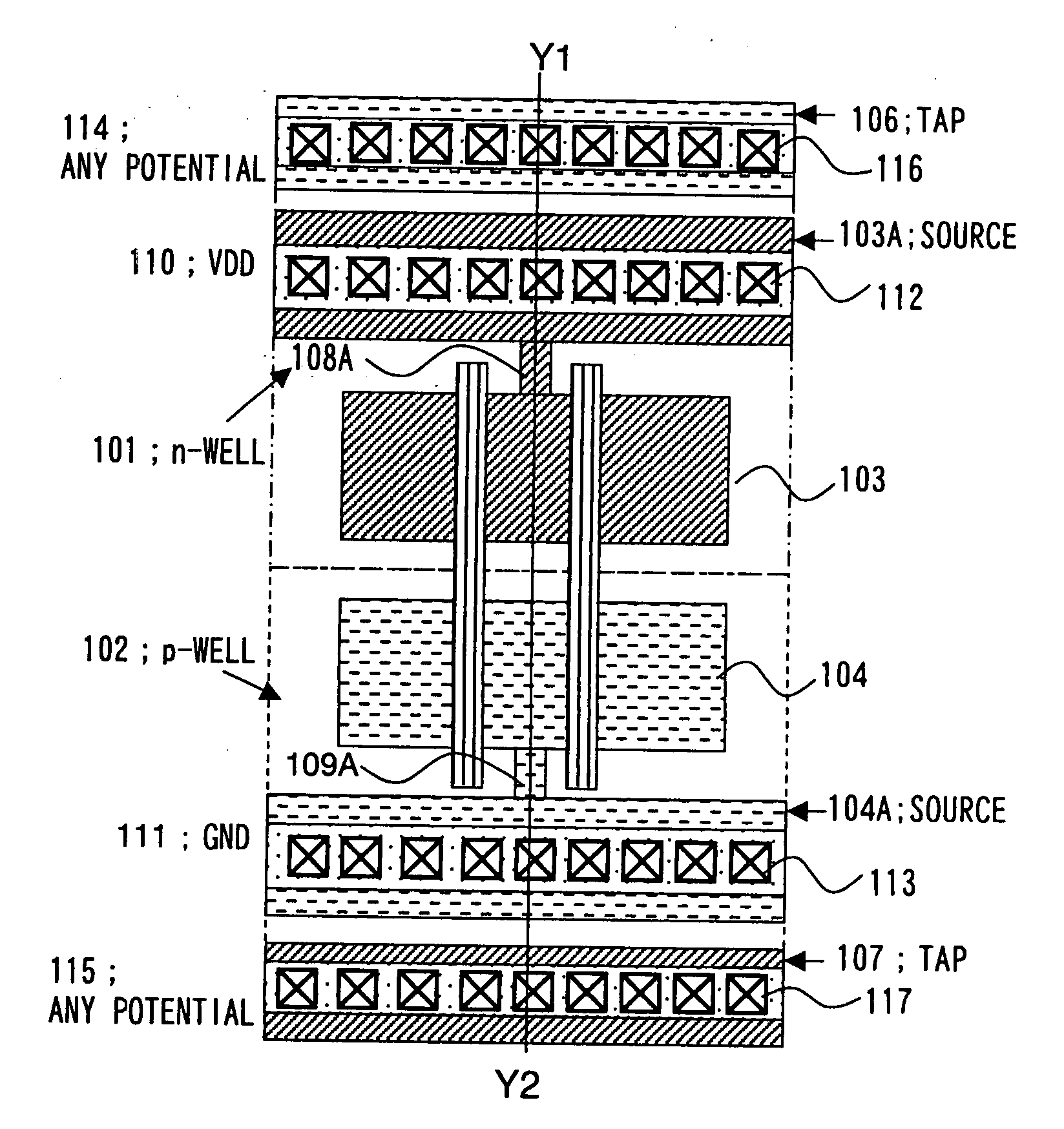
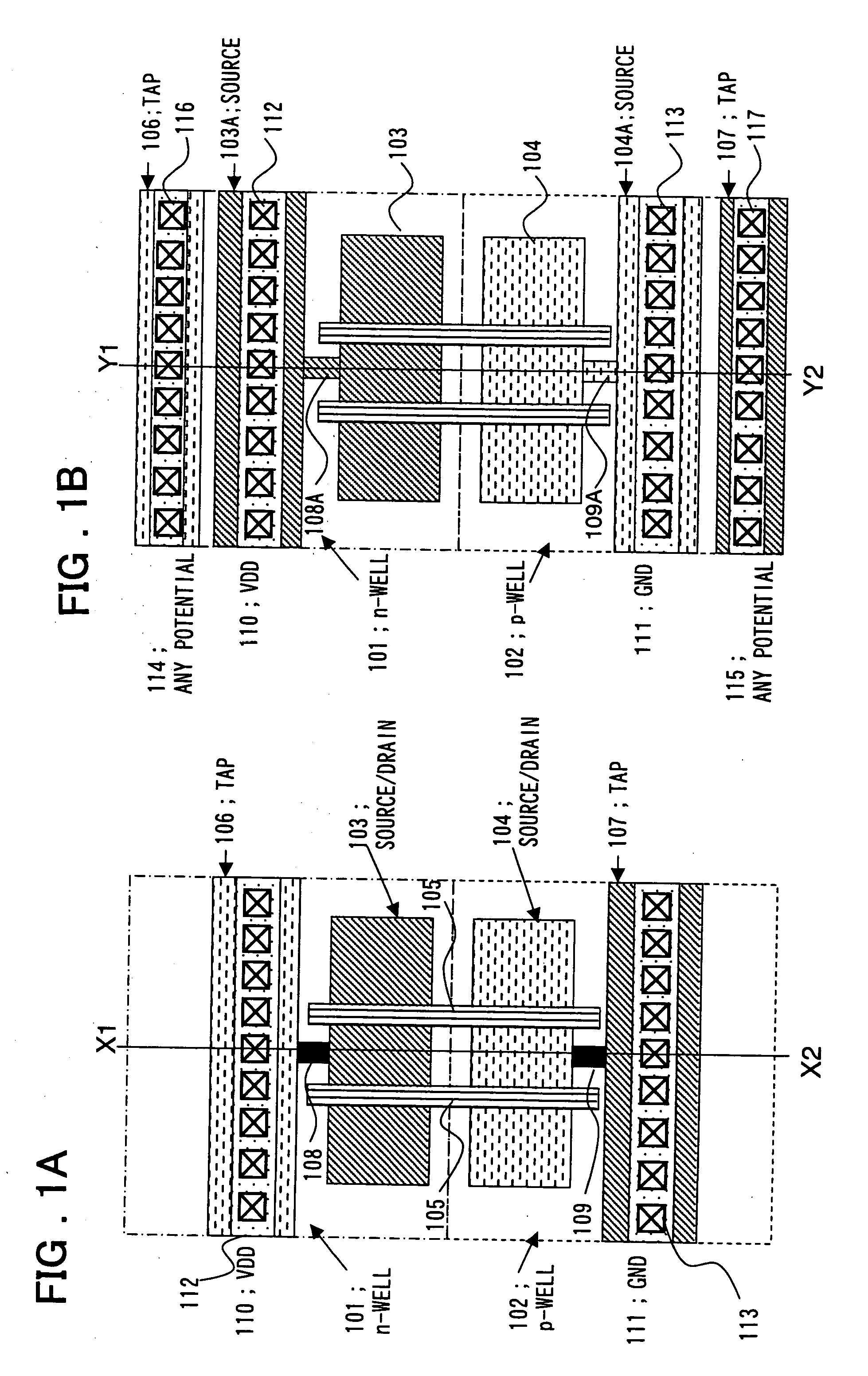
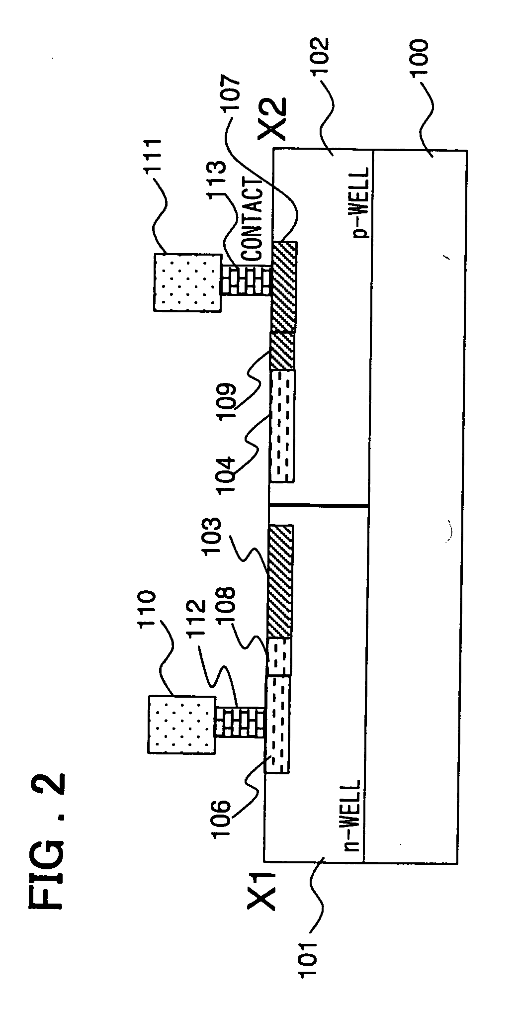
[0050] The present invention inputs a cell having taps, which supply the potentials of wells in which active elements are formed, provided in a semiconductor substrate surface, converts the taps of the cell to a conductivity type identical with that of a source diffusion region, adopts these taps as new source regions and sets the well potentials of the cell freely to any potentials. This will be described in detail in accordance with embodiments that follow below.

[0051]FIG. 1A is a diagram illustrating the structure of a cell in which well potential is fixed at power-supply potential (ground potential). Although there is no particular limitation, FIGS. 1A and 1B illustrate cells having a twin-well configuration in which a semiconductor substrate is provided with an n-well and a p-well. It goes without saying that the present invention is not limited to...


PUM


Abstract

Disclosed are a design method and apparatus in which information regarding a cell is input, the cell having taps in a substrate surface, for supplying the potentials of respective ones of wells in which active elements are formed, and source diffusion regions in the substrate surface, conductivity types thereof being opposite those of the wells. The taps are converted to conductivity types identical with those of the source diffusion regions to obtain source regions and freely set the well potentials of the cell to any potentials. If the cell is one having shorting portions electrically connecting taps and sources and the shorting portions are diffusion regions of the same conductivity type as that of the taps, then the shorting portions are converted to conductivity types identical with those of the source diffusion regions to obtain source regions.

Description

FIELD OF THE INVENTION [0001] This invention relates to a semiconductor integrated circuit device and to a method, apparatus and program for designing this semiconductor integrated circuit device. More particularly, the invention relates to a semiconductor integrated circuit device in accordance with the standard cell method, and to a method, apparatus and program for designing the cell. BACKGROUND OF THE INVENTION [0002] In layout design of a semiconductor device using a library of standard cells or the like, a technique used heretofore involves adopting the power-supply potential as the potential of a substrate or well or setting the substrate or well potential to a potential different from that of the power-supply voltage in order to control the threshold value of a MOS transistor. This technique relies upon a method in which a tap for supplying the well potential is placed within a cell or in which a tap cell is disposed appropriately between cell rows. The specification of Pate...

Claims


Application Information

Patent Timeline
IPC IPC(8): H01L27/10
CPCH01L27/11807
Inventor YAMAMOTO, HIROSHI
Owner RENESAS ELECTRONICS CORP
Features
  • Generate Ideas
  • Intellectual Property
  • Life Sciences
  • Materials
  • Tech Scout
  • Unparalleled Data Quality
  • Higher Quality Content
  • 60% Fewer Hallucinations
Learn More