Interposer, and multilayer printed wiring board

a multi-layer printed, interposer technology, applied in the direction of printed circuit aspects, printed circuit stress/warp reduction, electrical apparatus construction details, etc., can solve the problems of high-performance ic thereon, difficult to load a high frequency, resin becomes brittle, etc., to increase the diameter of the opening, the interposer is enlarged, and the effect of easy destruction

Inactive Publication Date: 2006-09-14
IBIDEN CO LTD
View PDF23 Cites 74 Cited by
  • Summary
  • Abstract
  • Description
  • Claims
  • Application Information

AI Technical Summary

Benefits of technology

[0005] The present invention has been achieved to solve the above-mentioned problem and therefore, an object of the invention is to provide an interposer capable of preventing generation of cracks due to thermal expansion or thermal contraction and supplying electricity to electronic components such as the IC chip stably and a multilayer printed wiring board equipped with the interposer.

Problems solved by technology

Because the ceramic package substrate utilizes metallized wiring obtained by baking, its resistance rises and dielectric constant of ceramic is high, and therefore, it is difficult to load a high frequency, high performance IC thereon.
If it contains air bubbles, the resin becomes brittle.

Method used


Image

  • Interposer, and multilayer printed wiring board
  • Interposer, and multilayer printed wiring board
  • Interposer, and multilayer printed wiring board

Examples


examples

1. Resin Made Package Substrate

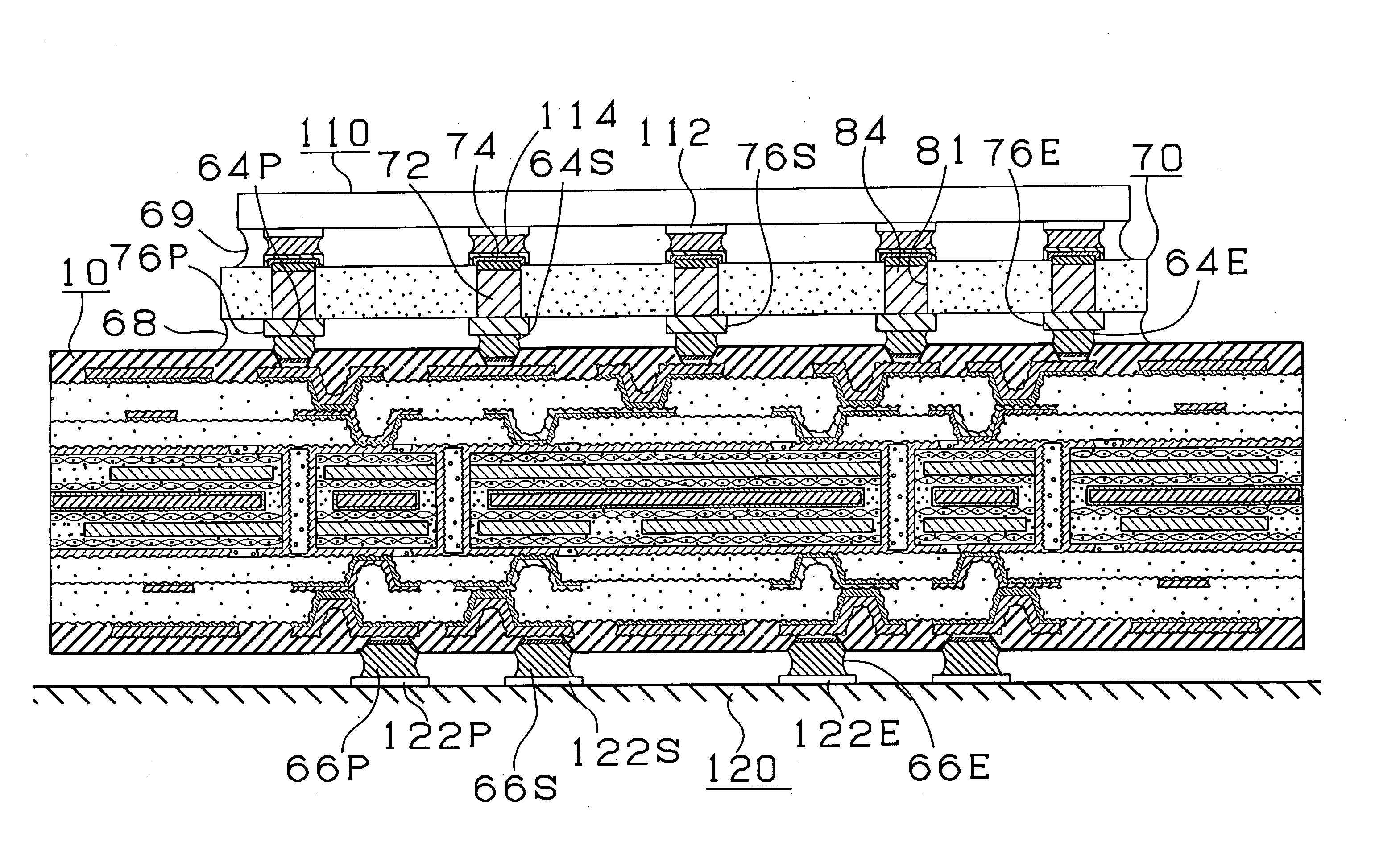
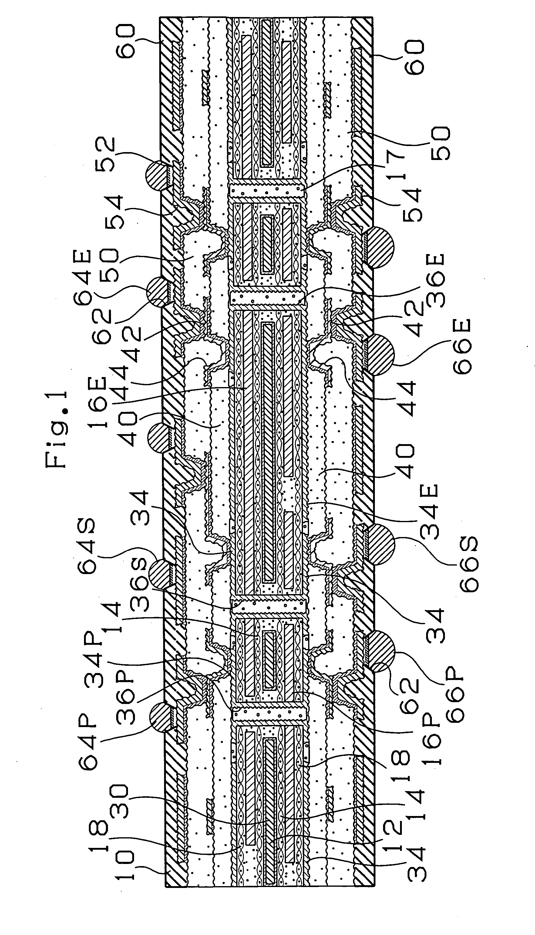
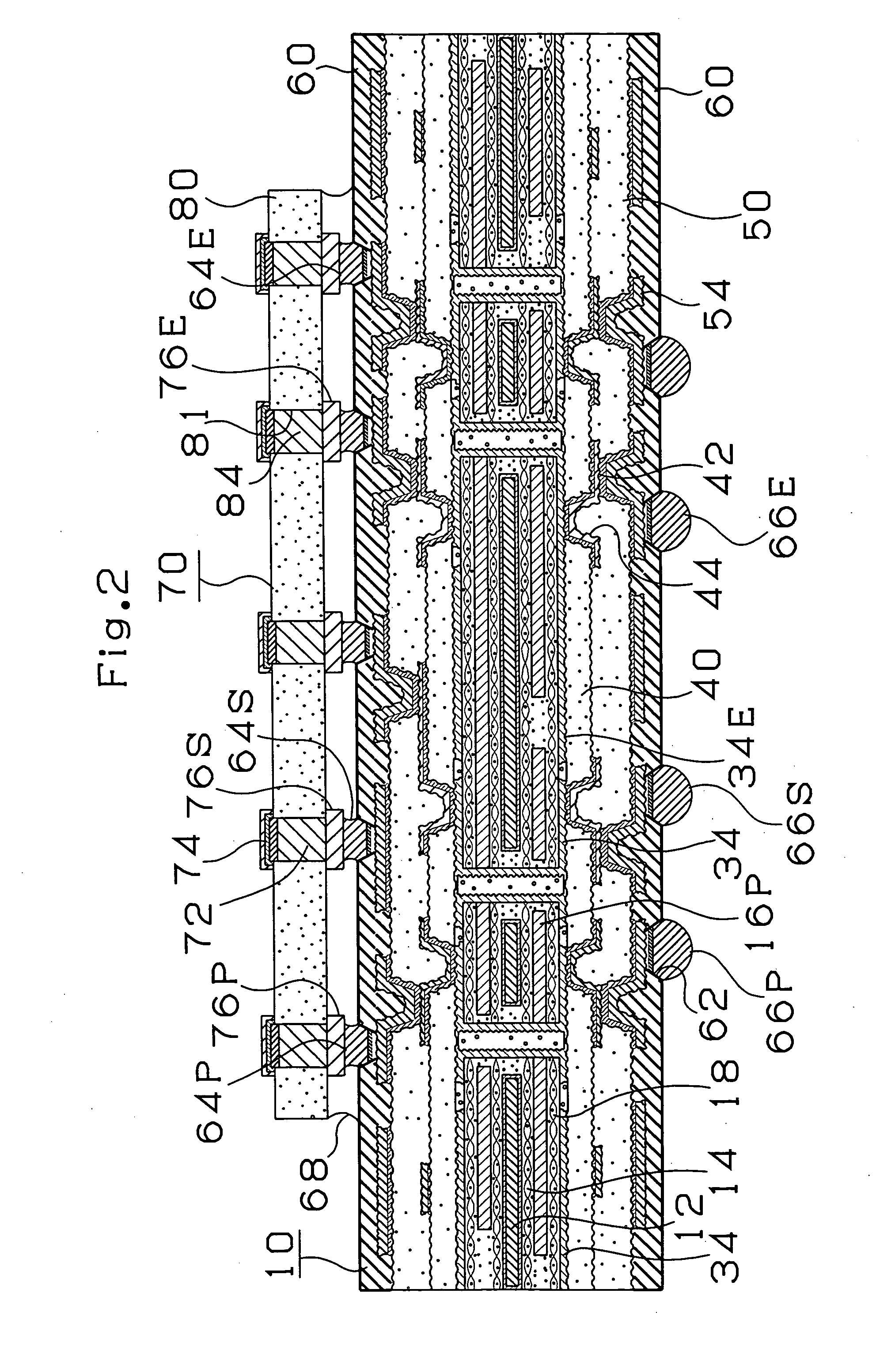
[0042] The structure of the resin made package substrate 10 will be described with reference to FIG. 1 showing a sectional view of the resin package substrate 10 according to the first example. The resin made package substrate 10 utilizes a multilayer core substrate 30. A conductor circuit 34 and conductive layer 34P are formed on the front surface side of the multilayer core substrate 30 and a conductor circuit 34 and conductive layer 34E are formed on the rear surface. The conductive layer 34P on the upper side is formed as a plain layer for power source and the conductive layer 34E on the lower side is formed as a plain layer for grounding. Further, a conductive layer 16E of an inner layer is formed on the upper face side inside the multilayer core substrate 30 and a conductive layer 16P is formed on the lower face side. The conductive layer 16E on the upper side is formed as a plain layer for grounding and the conductive layer 16P on the lower si...

first example

Young's Modulus=55 GPa, Dimension of External Shape=32 mm×32 mm, Thickness of Interposer=50 μm

[0054] The manufacturing process of the interposer of the first example will be described with reference to FIG. 6.

[0055] (1) 100 weight part of bisphenol A type epoxy resin, 5 weight part of imidazole type hardening agent and 60 weight part of alumina filler were mixed and that resin was impregnated into glass cloth and dried to obtain prepreg 80 as B stage. Hardened single face copper clad laminate 80A obtained by laminating the prepreg 80 and copper foil 78 and then pressing with heat under pressure was used as a starting material (FIG. 6(A)). The thickness of this insulating base material 80 is 50 μm and the thickness of the copper foil 78 is 12 μm. The Young's modulus of the insulating substrate constituting this interposer was 55 GPa when measured according to three-point-bending method based on JIS. In the meantime, for this measurement of Young's modulus, an insulating base materi...

second example

Young's Modulus=55 GPa, Dimensions of External Shape=32 mm×32 mm, Thickness of Interposer=64 μm

[0057] For the interposer of the second example, the thickness of the substrate of a starting material in the first example was set to 64 μm. Accompanied by that, laser condition for forming a through hole was changed to condition shown in the following table. Plating time for filling the through hole with conductive agent was changed corresponding to the thickness of the substrate. The other conditions were the same as the first example.

TABLE 2Laser conditionMask diameterF1.4mmPulse energy2.0mj / pulseShot count9shots


PUM


Abstract

An interposer capable of preventing breaking of a wiring pattern with an IC chip loaded on a package substrate. Stress due to a difference in thermal expansion coefficient between a multilayer printed wiring board having a large thermal expansion and the IC chip having a small thermal expansion can be absorbed by locating the interposer between the package substrate and the IC chip. Particularly by using an insulation substrate whose Young's modulus is 55 to 440 Gpa as the insulation substrate constituting the interposer, stress is absorbed within the interposer.

Description

BACKGROUND OF THE INVENTION [0001] The present invention relates to an interposer and a multilayer printed wiring board and more particularly to an interposer to be located between a package substrate made of resin and an IC chip made of ceramic and a multilayer printed wiring board equipped with an interposer for connecting the IC chip. [0002] The package substrate is used to connect the IC chip at a fine pitch to an external substrate such as daughter board. As material of the package substrate, ceramic or resin is used. Because the ceramic package substrate utilizes metallized wiring obtained by baking, its resistance rises and dielectric constant of ceramic is high, and therefore, it is difficult to load a high frequency, high performance IC thereon. On the other hand, the resin made package substrate allows its wiring resistance to be lowered because it utilizes copper wiring by plating and further, because dielectric constant of resin is low, loading of a high frequency, high ...

Claims


Application Information

Patent Timeline
Patent Type & Authority Applications(United States)
IPC IPC(8): H01L23/14H05K1/03H05K1/11H01L23/32H01L23/498H05K1/02H05K3/34
CPCH01L23/49827H01L2924/01019H01L2224/16H01L2924/01004H01L2924/01078H01L2924/01079H01L2924/09701H01L2924/15311H05K1/0271H05K1/0306H05K3/3436H05K3/4602H05K2201/10378H05K2201/10674H01L23/49833H01L2224/0554H01L2224/05568H01L2224/05573H01L2224/06131H01L2924/00014H01L2224/05599H01L2224/0555H01L2224/0556
Inventor KARIYA, TAKASHIFURUTANI, TOSHIKI
Owner IBIDEN CO LTD
Why Eureka
Try Eureka