Through electrode, package base having through electrode, and semiconductor chip having through electrode

Active Publication Date: 2006-09-14
TAIWAN SEMICON MFG CO LTD
6 Cites 41 Cited by

AI-Extracted Technical Summary

Problems solved by technology

Filling the electrode forming hole with the conductive body is time consuming, and therefore, the manufacturing efficiency of the through electrode manufacturing process is low.
This proble...

Benefits of technology

[0027] The inner volume of the electrode forming hole, in which the conductive body is embedded, is decreased, and therefore, the time necessary to embed the conductive body in the electrode forming hole is reduced. Consequently, the manufacturing efficiency of the through e...

Abstract

A through electrode extends through a silicon substrate from the upper surface to the lower surface of the substrate to accomplish electrical conduction between the upper and lower surfaces of the substrate. The through electrode includes a plurality of slender through holes formed in a through electrode forming area of the silicon substrate. The slender through holes extend through the silicon substrate from the upper surface to the lower surface of the silicon substrate. The through electrode also includes a plurality of conductive bodies fitted in the slender through holes. The conductive bodies are electrically connected with each other.

Application Domain

Technology Topic

Semiconductor chipElectrical conduction +2

Image

  • Through electrode, package base having through electrode, and semiconductor chip having through electrode
  • Through electrode, package base having through electrode, and semiconductor chip having through electrode
  • Through electrode, package base having through electrode, and semiconductor chip having through electrode

Examples

  • Experimental program(4)

Example

First Embodiment
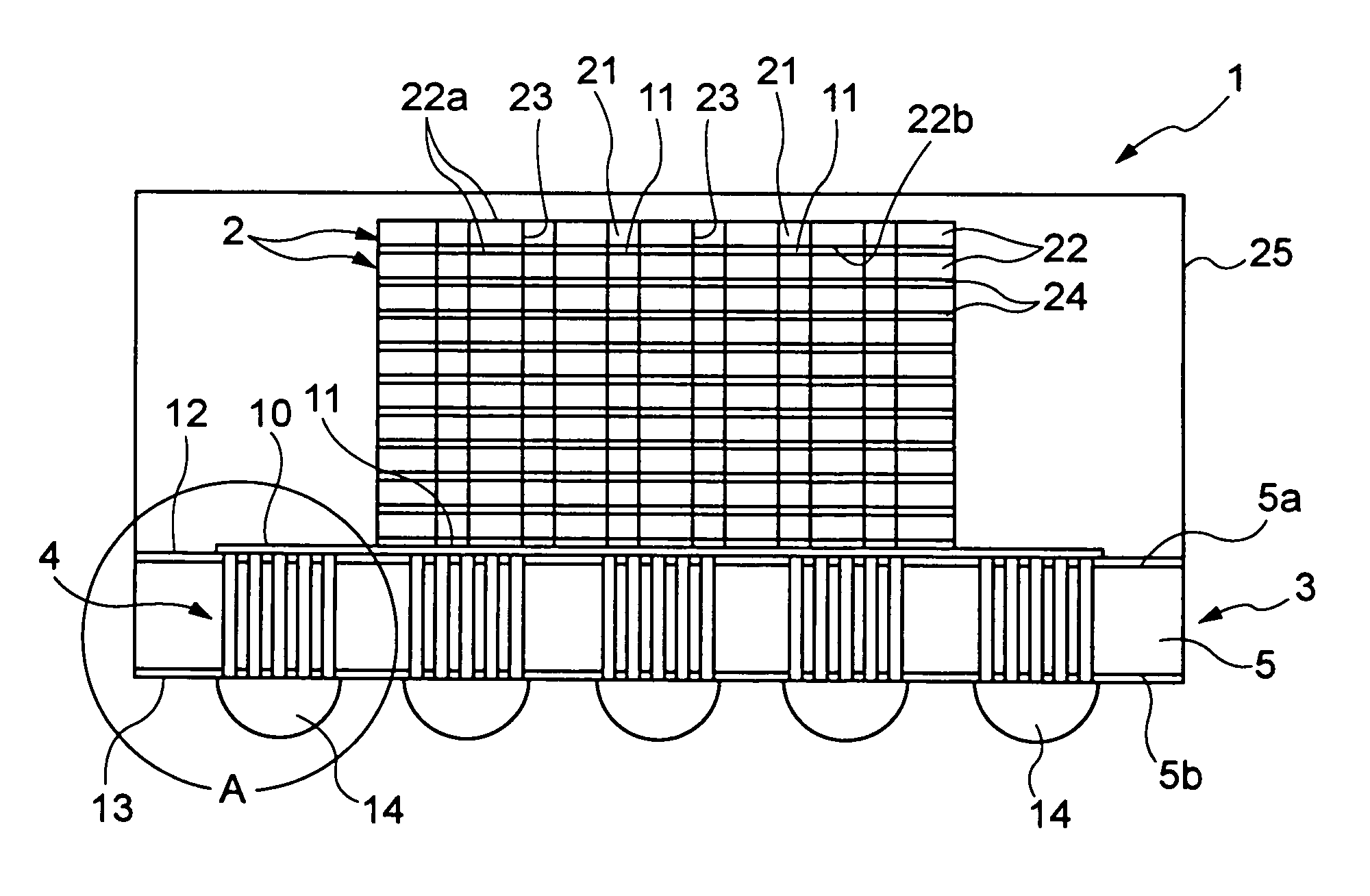
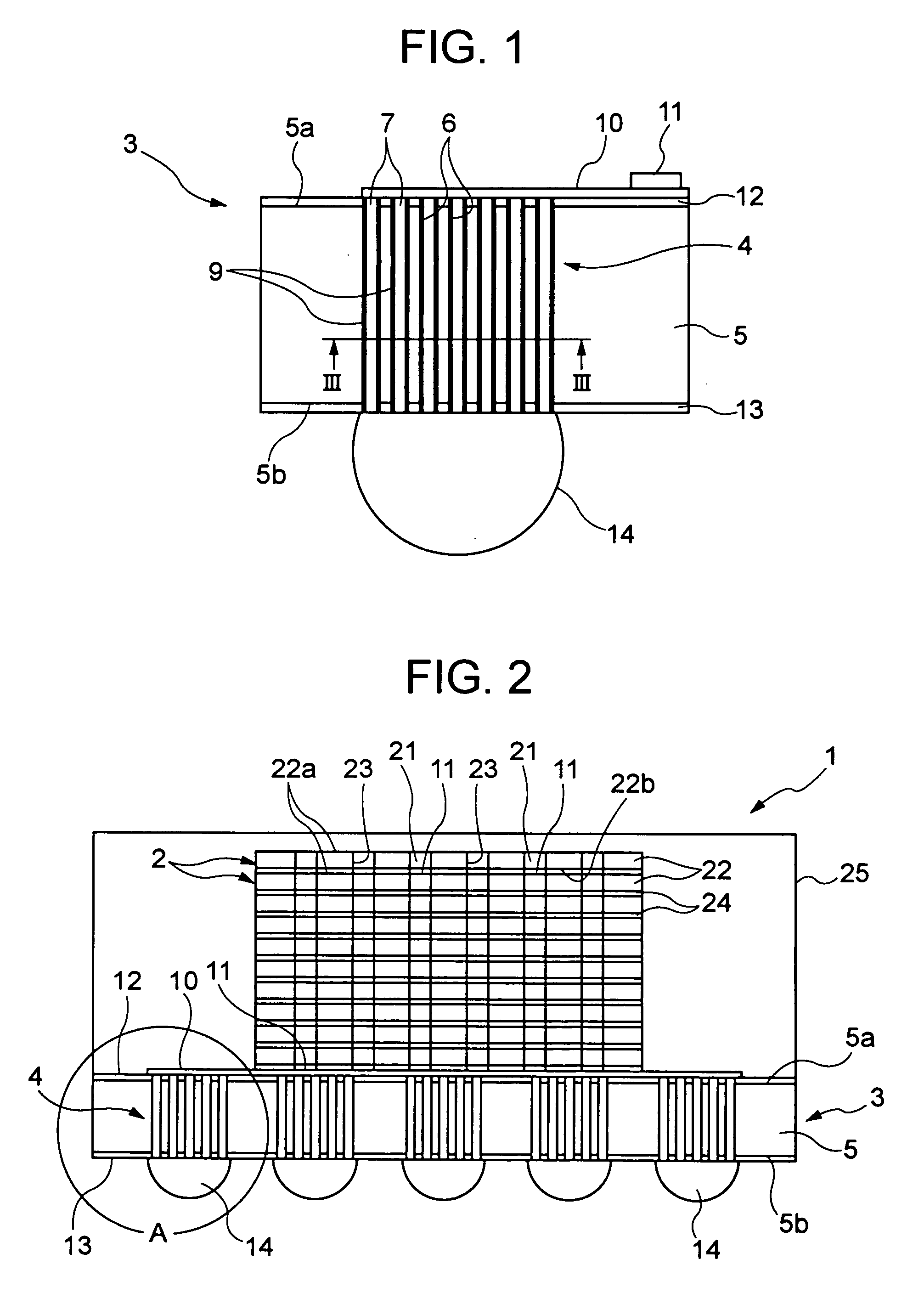
[0045] Referring to FIG. 1 to FIG. 3, a through electrode and a method of making the through electrode according to a first embodiment will be described. FIG. 1 is an enlarged view of part A in FIG. 2.
[0046] Referring to FIG. 2, a semiconductor package 1 includes a plurality of semiconductor chips 2 stacked one on another on a package base 3.
[0047] In FIG. 2, a plurality of through electrode units 4 are provided in the package base 3. Each through electrode unit 4 includes a plurality of slender conductive bodies 7 made of copper or silver. The conductive bodies 7 are embedded in a plurality of slender through holes 6 formed through a silicon substrate (i.e., base substrate) 5 of the package base 3 from the upper surface 5a to the lower surface 5b of the base substrate 5, respectively. The through electrode units 4 establish electrical conduction between the upper surface 5a and the lower surface 5b of the base substrate 5.
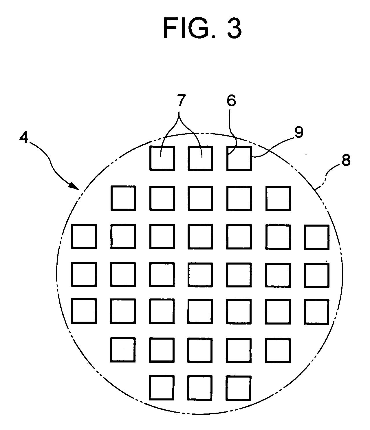
[0048] The through holes 6 have a square cross-sectional shape having a width of 5 to 30 μm or a circular cross-sectional shape having a diameter of 5 to 30 μm. The through holes 6 are provided in each of through electrode forming areas 8. FIG. 3 shows one through electrode forming area 8 by a two-dot chain line.
[0049] Each through electrode forming area 8 is a circular area and has a diameter approximately equal to that of an external terminal 14. Each through electrode forming area 8 is located at the position where the associated through electrode unit 4 is formed.
[0050] Insulating films 9 made of silicon dioxide are also provided in the through holes 6. Each insulating film 9 is disposed between the side wall of each through hole 6 and the corresponding conductive body 7 for electrically insulating the conductor body 7 and the base substrate 5 from each other. In FIGS. 1 and 3, the insulating films 9 are shown by a solid bold line.
[0051] A rerouting wire 10 is constituted by a wiring pattern formed on the upper surface 5a of the base substrate 5. The rerouting wire 10 has one end joined to the upper surface of the through electrode unit 4 and the other end joined to a bump 11. The bump 11 is formed at a bump forming area and joined to a conductive plug 21 of the semiconductor chip 2 connected to the through electrode unit 4. Consequently, the through electrode unit 4 and the bump 11 are electrically connected by the rerouting wire 10.
[0052] The bump 11 is formed by applying a bump material containing nickel (Ni) and gold (Au) in a paste state at the bump forming area on the rerouting wire 10 by potting, and then thermally hardening the applied bump material. The bump material may contain copper and tin-silver alloy, instead of nickel and gold. Alternatively the bump material may contain copper alone.
[0053] An upper face insulating layer 12 made of insulating material, such as silicon dioxide or silicon nitride (Si3N4), is formed on the upper surface 5a of the base substrate 5 except for the upper ends of the conductor bodies 7. The upper insulating layer 12 electrically insulates the rerouting wire 10 and the base substrate 5 from each other.
[0054] A lower face insulating layer 13 made of an insulating material, such as silicon dioxide or silicon nitride, is formed on the lower surface 5b of the base substrate 5 except for the lower ends of the conductor bodies 7. The lower insulating layer 13 electrically insulates a mounting substrate (not shown) and the base substrate 5 from each other.
[0055] A plurality of external terminals 14 are provided on the lower surface 5b of the base substrate 5. Each external terminal 14 is made of tin-lead alloy or tin-silver alloy, and has a relatively large inner diameter (for example, approximately Φ 300 μm). The external terminal 14 is joined to the lower ends of the conductive bodies 7 of each through electrode unit 4. The external terminals 14 are located at the positions corresponding to wire terminals of the mounting substrate (not shown) to electrically connect the semiconductor package 1 to the mounting substrate.
[0056] It should be noted that the lower insulating layer 13 may be omitted so long as the electrical insulation between the mounting substrate and the base substrate 5 is not affected.
[0057] Also, the upper surface 5a of the base substrate 5 excluding the bumps 11 may be coated with a coating material, such as polyimide, as occasion demands, to protect the rerouting wire 10 and electrically insulate the rerouting wire 10 from the semiconductor chip 2.
[0058] Referring to FIG. 2, conductive plugs 21 serve as through electrodes of each semiconductor chip 2. Each conductive plug 21 is formed by embedding the conductive body 7 in each chip through hole 23 extending through the semiconductor chip 2 from the upper surface 22a of the silicon substrate (i.e., chip substrate) 22 of each semiconductor chip 2 to the lower surface 22b of the chip substrate 22. Circuit elements are formed on the chip substrate upper surface 22a. Circuit elements are not formed on the chip substrate lower surface 22b. The electrical conduction between the upper and lower surfaces 22a and 22b of the chip substrate 22 is accomplished by the conductive plugs 21.
[0059] The bumps 11 are directly provided at the upper ends of the conductive plugs 21 embedded in each of the chip substrates 22 below the uppermost chip substrate 22.
[0060] Under-fills 24 are formed between each two semiconductor chips 2 and between the lowest semiconductor chip 2 and package substrate 3. Each under-fill 24 is created by injecting an under-filling material, such as epoxy resin, between the respective semiconductor chips 2 and between the lowermost semiconductor chip 2 and the package base 3, excluding the bumps 11, and thermally hardening the injected under-fill material. The protection and electrical insulation between the respective semiconductor chips 2 are accomplished by the under-fills 24.
[0061] An over-mold 25 is formed by providing a molding material, such as epoxy resin, over the upper surface 3a of the package base 3. The molding material encloses (buries) the stacked semiconductor chips 2 and is thermally hardened. The over-mold 25 serves to protect the semiconductor chips 2 and the rerouting wires 10 from the outside.
[0062] The over-mold 25 is formed by transfer molding. Specifically, the semiconductor chips 2 are stacked on a plurality of package bases 3 formed on a wafer, or the wafer is divided into a plurality of elongated rectangle shapes having a plurality of package bases 3, and then the semiconductor chips 2 are stacked on the package bases 3. Subsequently, the semiconductor chips 2 stacked on the package bases 3 are placed in a mold having a predetermined size, and the mold is filled with the molding material to form the over-mold 25.
[0063] When the semiconductor chips 2 are stacked one on another on the package base 3 and then joined to the package base 3, the lower ends of the conductive plugs 21 of the lowermost (first) semiconductor chip 2 are aligned with the bumps 11 on the rerouting wires 10 of the package base 3, and then the lower ends of the conductive plugs 21 of the next (second) semiconductor chip 2 are aligned with the bumps 11 on the upper ends of the conductive plugs 21 of the lowermost semiconductor chip 2. This aligning and stacking is repeated for subsequent semiconductor chips 2. Then, the bumps 11 are melted by heat to join the conductive plugs 21 of the semiconductor chips 2, and, at the same time, to join the conductive plugs 21 to the rerouting wires 10 of the package base 3. Consequently, the conductive plugs 21 of each semiconductor chip 2 and the external terminals 14 of the package base 3 are electrically connected with each other, and the conductive plugs 21 disposed at a narrow interval are electrically connected to the wire terminals of the mounting substrate (not shown), which are disposed at a relatively wide interval, via the external terminals 14.
[0064]FIGS. 4A to 4E are sectional views illustrating a package base manufacturing method according to a first embodiment of the present invention.
[0065] Referring to FIG. 4A, a plurality of slender electrode forming holes 15 which will later become the slender through holes 6 are formed in the upper surface 5a of the base substrate 5. Each slender electrode forming hole 15 has a bottom.
[0066] The depth of each electrode forming hole 15 is not less than 7% and not greater than 27% of the thickness of the base substrate 5. Preferably, the depth of the narrow electrode forming hole 15 is approximately 20% of the thickness of the base substrate 5. If the depth of the electrode forming holes 15 is less than 7% of the thickness of the base substrate 5, the thickness of the base substrate 5 becomes excessively small as the base substrate 5 is thinned at the process P5, and therefore, the strength of the package substrate 1 is significantly reduced. If the depth of the electrode forming hole 15 is greater than 27% of the thickness of the base substrate 5, the ratio of the inner diameter to the depth of the electrode forming hole 15 is excessively increased, and therefore, it becomes difficult to form an insulating film 9 at the process P2. Thus, it is preferred that the depth of each electrode forming hole 15 be approximately 20% of the thickness of the base substrate 5.
[0067] A mask pattern 18 is similar to the mask pattern 125.
[0068] Now, the package base manufacturing method according to the first embodiment of the present invention will be described based on the processes P1 (FIG. 4A) to P5 (FIG. 4E).
[0069] At the process P1 (FIG. 4A), columnar silicon is sliced to form a silicon substrate, i.e., a base substrate 5. Thereafter, a mask pattern 18 is applied to the upper surface 5a of the base substrate 5 except for through hole forming areas of the through electrode forming areas 8, and the through electrode forming areas 8 are dry-etched to form the electrode forming holes 15 having a predetermined depth.
[0070] The electrode forming holes 15 may be formed by laser. The laser makes it possible to directly form the electrode forming holes 15 in the base substrate 5 without using the mask pattern 18.
[0071] At the process P2 (FIG. 4B), the mask pattern 18 is removed, and an upper insulating layer 12 and an insulating film 9, both made of silicon dioxide, are formed on the upper surface 5a of the base substrate 5 and on the inner walls of the electrode forming holes 15, respectively, by CVD.
[0072] At the process P3 (FIG. 4C), conductive bodies 7 are embedded in the electrode forming holes 15, such that the inner volumes of the electrode forming holes 15 surrounded by the insulating film 9 are filled with the conductive bodies, by plating.
[0073] At the process P4 (FIG. 4D), a resist mask is formed on the upper insulating layer 12 by lithography to mask the upper insulating layer 12 except for a rerouting wire forming area. The rerouting wire 10 is formed on the exposed part of the upper insulating layer 12 by the plating such that the rerouting wire 10 extends from the top of the through electrode unit 4 to the bump 11.
[0074] Subsequently, the resist mask is removed by a detaching agent, and then a bump material 10 is applied to the bump forming area on the rerouting wire 10 by potting. After that, the bump material 10 is thermally hardened. As a result, the bump 11 is formed.
[0075] At the process P5 (FIG. 4E), the lower surface 5b of the base substrate 5 is removed by mechanical grinding or chemical mechanical polishing (CMP), and the base substrate 5 is thinned such that the conductive bodies 7 are exposed at the lower surface 5b of the base substrate 5. A lower insulating layer 13, which is made of silicon dioxide, is then formed on the lower surface 5b of the base substrate 5 by CVD.
[0076] Subsequently, those portions of the lower insulating layer 13, which are formed at the lower ends of the conductive bodies 7, are removed by CMP, and then an external terminal 14 is joined to the exposed lower ends of the conductive bodies 7 by soldering with a tin-lead alloy ball.
[0077] As a result, the conductive bodies 7, which are embedded in the through holes 6, constitute the through electrode unit 4 in the first embodiment of the present invention. The through electrode unit 4 serves as a through electrode that establishes electrical conduction between the upper surface 5a and the lower surface 5b of the base substrate 5.
[0078] In this way, a wafer having a plurality of package bases 3 is manufactured in the first embodiment.
[0079] If the package bases 3 are individually used, the wafer is divided into the individual package bases 3.
[0080] If the semiconductor package 1 is manufactured using the wafer having the package bases 3, the lower surfaces of the conductive plugs 21 of the lowermost one of the separately-prepared semiconductor chips 2, which are stacked via the bumps 11, are placed on the bumps 11 of the rerouting wires 10 of the package bases 3, and the bumps 11 are melted by heating. As a result, the conductive plugs of the respective semiconductor chips 2 are joined with each other, and the conductive plugs 21 of the lowermost semiconductor chip 2 and the rerouting wires 10 are also joined with each other.
[0081] Subsequently, under-filling materials are injected between the respective semiconductor chips 2, and are then thermally hardened to form the under-fills 24. After that, a molding material is supplied over the upper surface 5a of the base substrate 5 by transfer molding such that the stacked semiconductor chips 5 are buried in the molding material. The molding material is thermally hardened to form the over-mold 25.
[0082] Thereafter, the wafer is divided into individual package bases 3 to obtain the semiconductor package 1.
[0083] As described above, the conductive bodies are embedded in the through holes formed in the upper surface of the base substrate in the first embodiment, and therefore, the total inner volume of the through holes to be filled with the conductive bodies is decreased, and the time necessary to embed the conductive body is reduced. Consequently, the efficiency of the through electrode manufacturing process increases. Also, the external terminal is joined to the through electrode unit constituted by the slender electrodes so that satisfactory joining strength is ensured between the external terminal and the through electrode unit.

Example

Second Embodiment
[0084]FIG. 5 is a partial sectional view illustrating a package base according to a second embodiment of the present invention, and FIG. 6 is a cross-sectional view taken along line VI-VI in FIG. 5.
[0085] Components of the package base in the second embodiment, which are identical to those of the package base in the first embodiment, are indicated by the same reference numerals as the first embodiment, and a description thereof will not be given.
[0086] Referring to FIGS. 5 and 6, an electrode unit through hole 31 has the same dimension as the electrode forming area 8. In the electrode unit through hole 31 are disposed a plurality of silicon columns 32. Each silicon column 32 has a square sectional shape having a width of 5 to 30 μm or a circular sectional shape having a diameter of 5 to 30 μm. The electrode unit through hole 31 except for the silicon columns 32 is filled with a conductive body 7 to form a lotus root-shaped through electrode unit 4. In FIGS. 5 and 6, insulating films 9 are shown by a solid bold line.
[0087]FIGS. 7A to 7E are cross-sectional views illustrating a package base manufacturing method according to the second embodiment of the present invention.
[0088] Referring to FIGS. 7A to 7E, an electrode unit forming hole 33 will later become the electrode unit through hole 31. The electrode unit forming hole 33 is formed in the upper surface 5a of the base substrate 5. The electrode unit forming hole 33 has the same depth as the electrode forming holes 15 of the first embodiment, and has a bottom. The silicon columns 32 stand upright from the bottom of the electrode unit forming hole 33.
[0089] For the purpose of clarity, only one of the silicon columns 32 is shown in FIGS. 7A to 7E.
[0090] Now, the package base manufacturing method according to the second embodiment will be described based on processes PA1 (FIG. 7A) to PA7 (FIG. 7E).
[0091] At the process PA1 (FIG. 7A), a base substrate 5, which is the same as the base substrate formed at the process P1 according to the first embodiment, is prepared. Thereafter, a mask pattern 18 is applied to the upper surface 5a of the base substrate 5 except for a through electrode forming area 8 and also applied to silicon column forming areas in the through electrode forming area 8. The through electrode forming area 8 is dry-etched to form an electrode unit forming hole 33, which has a predetermined depth and has silicon columns 32 standing uprightly on the bottom of the electrode unit forming hole 33.
[0092] The electrode unit forming hole 33 may be formed by laser. The laser makes it possible to directly form the electrode unit forming hole 33 in the base substrate 5 without using the mask pattern 18.
[0093] At the process PA2 (FIG. 7B), an upper face insulating layer 12 and an insulating film 9 are formed on the upper surface 5a of the base substrate 5, the inner wall of the electrode unit forming hole 33, and the side and top surfaces of the silicon columns 32, respectively, in the same manner as the process P2 of the first embodiment.
[0094] At the process PA3 (FIG. 7C), a conductive body 7 is embedded in the electrode unit forming hole 33 in the same manner as the process P3 of the first embodiment. The inner volume of the electrode unit forming hole 33 is filled with the conductive body 7.
[0095] At the process PA4 (FIG. 7D), a rerouting wire 10 is formed on the upper insulating layer 12 such that the rerouting wire 10 extends from the top of the through electrode unit 4 to a bump 11, and then the bump 11 is formed. The process PA4 is carried out in the same manner as the process P4 according to the first embodiment of the present invention.
[0096] At the process PA5 (FIG. 7E), a lower insulating layer 13 is formed on the lower surface 5b of the base substrate 5, that portion of the lower insulating layer 13, which is formed at the lower end surface of the conductive body 7, is removed, and then an external terminal 14 is joined to the lower end surface of the conductive body 7, in the same manner as the process P5 of the first embodiment.
[0097] As a result, the lotus root-shaped conductive body 7, which is formed by providing the silicon columns 32 in the electrode unit through hole 31, constitutes the through electrode unit 4 of the second embodiment. The through electrode unit 4 establishes electrical conduction between the upper surface 5a and the lower surface 5b of the base substrate 5.
[0098] In this way, a wafer having a plurality of package bases 3 is manufactured according to the manufacturing method of the second embodiment.
[0099] The subsequent processes in the case where the package bases 3 are individually used and in the case where the semiconductor package 1 is manufactured using the wafer having a plurality of package bases 3 are the same as in the first embodiment, and therefore, a description thereof will not be given.
[0100] As described above, the second embodiment of the present invention has the same advantages as the first embodiment. In addition, because the through electrode unit is formed in the shape of a lotus root in the second embodiment, the joining area between the through electrode unit and the external terminal is increased, and therefore, the joining strength between the through electrode unit and the external terminal is further enhanced.

Example

Third Embodiment
[0101]FIG. 8 is a partial sectional view illustrating a package base according to a third embodiment of the present invention.
[0102] Components of the package base according to the third embodiment, which are identical to those of the package base according to the first embodiment, are indicated by the same reference numerals as those of the package base according to the first embodiment, and a description thereof will not be given.
[0103] A through electrode unit 4 in the third embodiment is the same as the through electrode unit in the first embodiment.
[0104] Referring to FIG. 8, a pad 35 made of copper or nickel and gold is formed in the through electrode forming area 8 such that the lower ends of a plurality of conductive bodies 7 of the through electrode unit 4 are joined with each other by the pad 35. In FIG. 8, insulating films 9 are shown by a solid bold line.
[0105] Now, the package base manufacturing method according to the third embodiment of the present invention will be described based on processes PB1 (FIG. 9A) to PB5 (FIG. 9E).
[0106] The process PB1 to the process PB4 in the third embodiment are the same as the process P1 to the process P4 in the first embodiment, and therefore, a description thereof will not be given.
[0107] At the process PB5 (FIG. 9E), a lower insulating layer 13 is formed on the lower surface 5b of the base substrate 5, and those portions of the lower insulating layer 13, which are formed at the lower ends of the conductive bodies 7, are removed, in the same manner as the process P5 of the first embodiment. Subsequently, a pad 35 is formed over the through electrode forming area 8, including the lower ends of the conductive bodies 7 constituting the through electrode unit 4, by plating, such that the respective conductive bodies 7 are joined to each other by the pad 35, and then an external terminal 14 is joined to the pad 35 in the same manner as the process P5 of the first embodiment.
[0108] As a result, the conductive bodies 7, which are embedded in the through holes 6, constitute the through electrode unit 4 in this embodiment of the present invention. The through electrode unit 4 establishes electrical conduction between the upper surface 5a and the lower surface 5b of the base substrate 5. Also, the slim conductive bodies 7 are joined with each other by the pad 35.
[0109] In this way, a wafer having a plurality of package bases 3 is manufactured according to the manufacturing method of the third embodiment.
[0110] The subsequent processes in the case where the package bases 3 are individually used and in the case where the semiconductor package 1 is manufactured using the wafer having the package bases 3 are the same as in the first embodiment, and therefore, a description thereof will not be given.
[0111] As understood from the foregoing, the third embodiment has the same advantage as the first embodiment. In addition, because the narrow conductive bodies are joined with each other by the pad, the joining area between the through electrode unit and the external terminal is increased, and therefore, the joining strength between the through electrode unit and the external terminal is further enhanced.

PUM

no PUM

Description & Claims & Application Information

We can also present the details of the Description, Claims and Application information to help users get a comprehensive understanding of the technical details of the patent, such as background art, summary of invention, brief description of drawings, description of embodiments, and other original content. On the other hand, users can also determine the specific scope of protection of the technology through the list of claims; as well as understand the changes in the life cycle of the technology with the presentation of the patent timeline. Login to view more.

Similar technology patents

Centrifuge Loading Process Within An Automated Laboratory System

ActiveUS20090318276A1Reduce timeDispersed particle separationCentrifugal force sediment separationEngineeringTime to result
Owner:SIEMENS HEALTHCARE DIAGNOSTICS INC

Classification and recommendation of technical efficacy words

  • Improve manufacturing efficiency
  • Reduce time

Rimless spectacles

InactiveUS20080198323A1Difficult to manufactureImprove manufacturing efficiencyLens assembliesLens plateElectrical and Electronics engineering
Owner:DONGGUAN JI SHENG OPTICAL

Trocar system and method of use

InactiveUS20080009797A1Improve manufacturing efficiencyFacilitate punctureInfusion syringesSurgical needlesAbdominal trocarEngineering
Owner:UNITED STATES SURGICAL CORP

3D printing method for building beam component

Owner:无锡华工大光电智能科技有限公司

Multi-component vascular device

ActiveUS20090099647A1Reduce timeReduce inventoryStentsDiagnosticsBody organsTreating Site
Owner:ST JUDE MEDICAL CARDIOLOGY DIV
Why Eureka
Try Eureka