

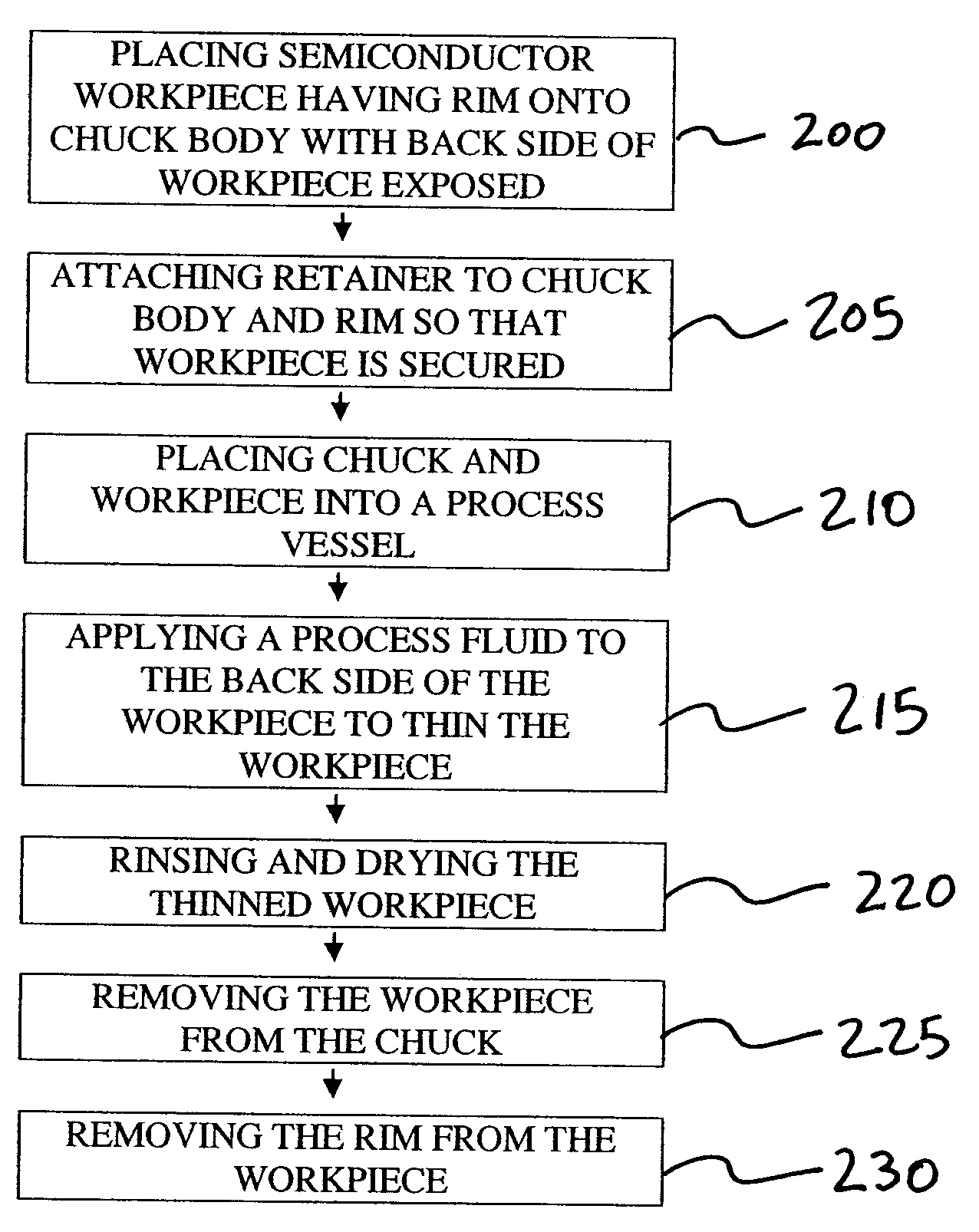
Process and apparatus for thinning a semiconductor workpiece
a technology for thinning workpieces and semiconductors, applied in electrical apparatus, semiconductor devices, basic electric elements, etc., can solve the problems of icds operating at extremely high speeds, prone to heat generation, and drawbacks of conventional back grinding processes, so as to reduce the number of processing steps, and improve yield
- Summary
- Abstract
- Description
- Claims
- Application Information
AI Technical Summary
Benefits of technology
Problems solved by technology
Method used
Image

Examples
Embodiment Construction
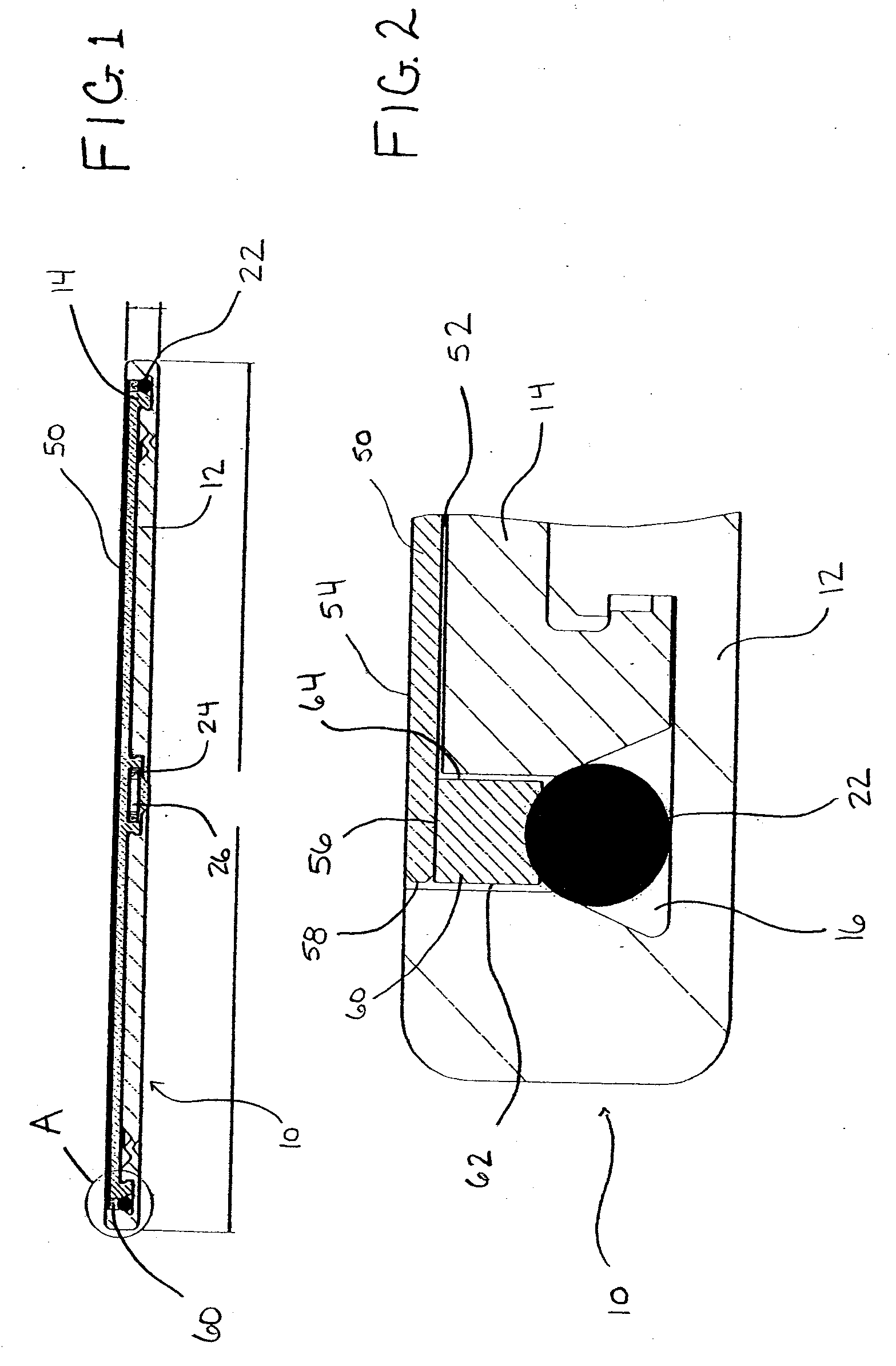
[0039] With reference to FIGS. 1-6, there is shown a chuck 10 for supporting a workpiece 50 during processing in accordance with one embodiment of the present invention. In accordance with the embodiment, the chuck 10 is comprised of an outer body 12 removably engaged to an inner body 14. When engaged, the outer body 12 and inner body 14 define a groove 16 around a peripheral portion of the chuck 10. The groove 16 houses an annular gasket 22 and accepts the polymer rim 60 that is bonded to the workpiece 50. A vacuum must be applied to secure the workpiece 50 to the chuck 10.
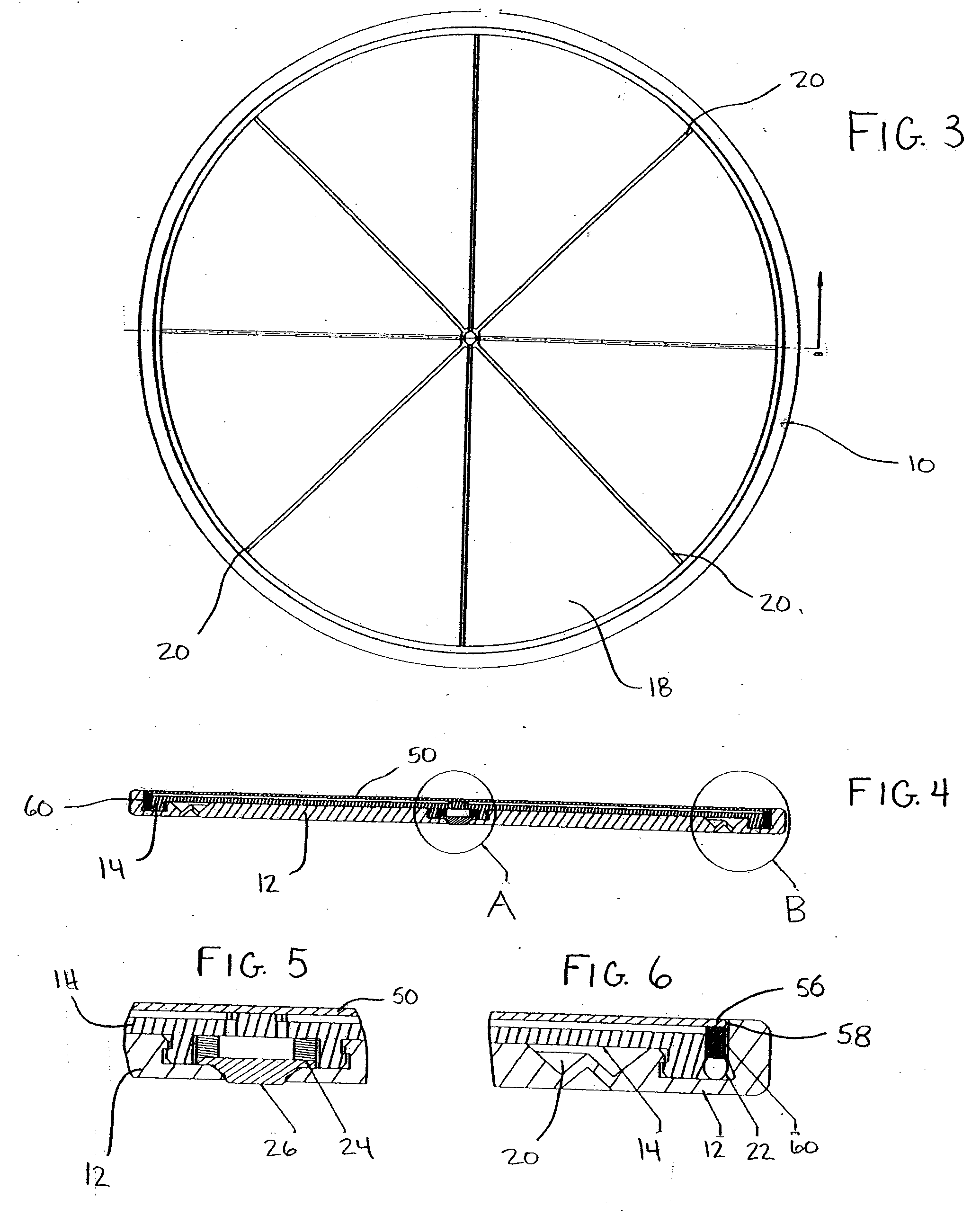
[0040] As best illustrated in FIG. 3, the chuck 10 of present invention has a cylindrical shape. The top of the chuck body 18 includes a series of channels 20 which communicate a vacuum to the workpiece, thus creating a seal between the workpiece and the inner body 14 of the chuck 10. The chuck 10 further comprises an annular gasket 22 formed from a compressible material to create a seal between the polymer rim ...
PUM
 Abstract
Description
Claims
Application Information