

Method for forming dual damascene with improved etch profiles
a technology of etching profiles and damascenes, which is applied in the direction of semiconductor/solid-state device manufacturing, basic electric elements, electric apparatus, etc., can solve the problems of reducing the size of the device, and affecting the quality of the etching profile. , to achieve the effect of improving the etching profile relative to the smaller device dimension, reducing the difficulty of providing interconnection technology, and improving the quality of the etch
- Summary
- Abstract
- Description
- Claims
- Application Information
AI Technical Summary
Benefits of technology
Problems solved by technology
Method used
Image

Examples
Embodiment Construction
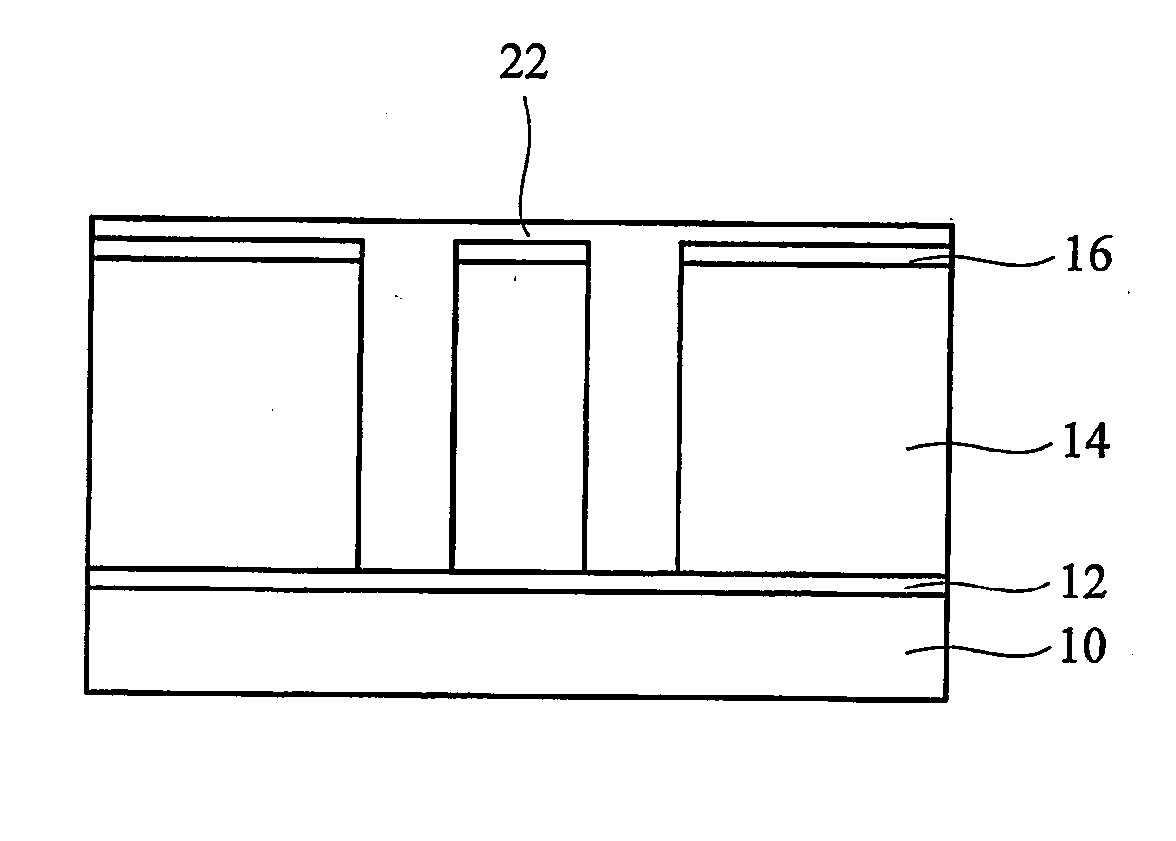
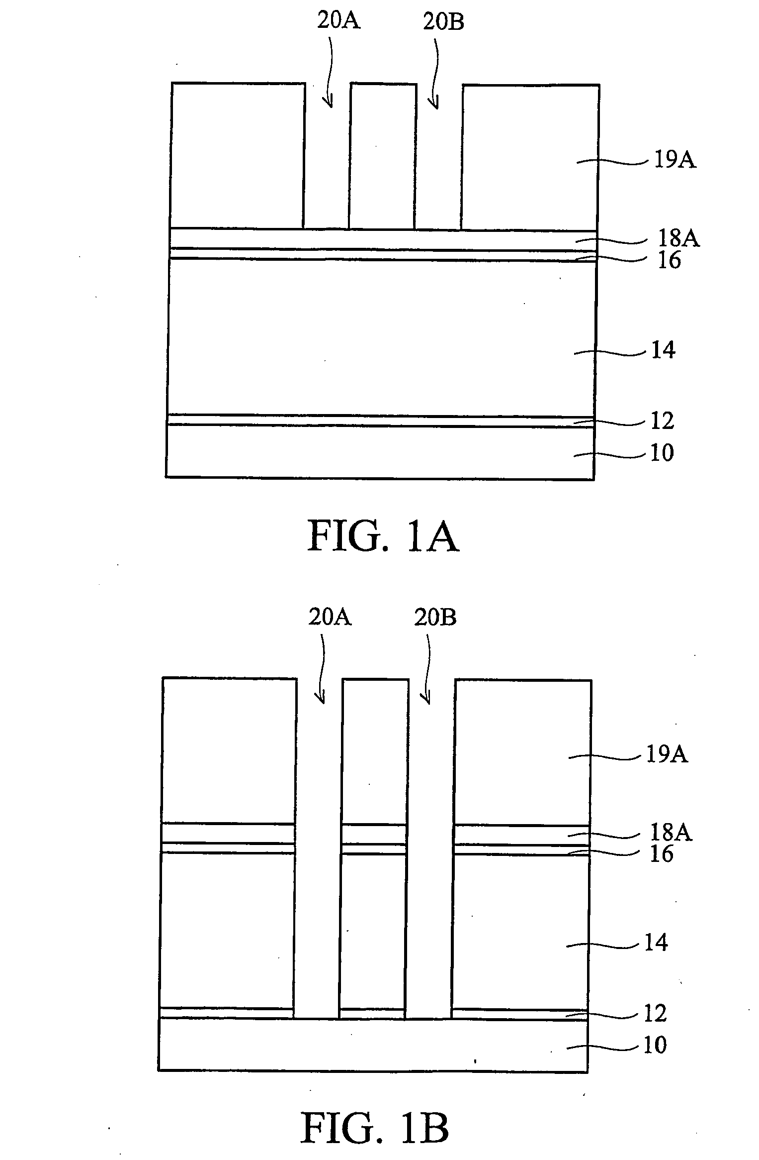
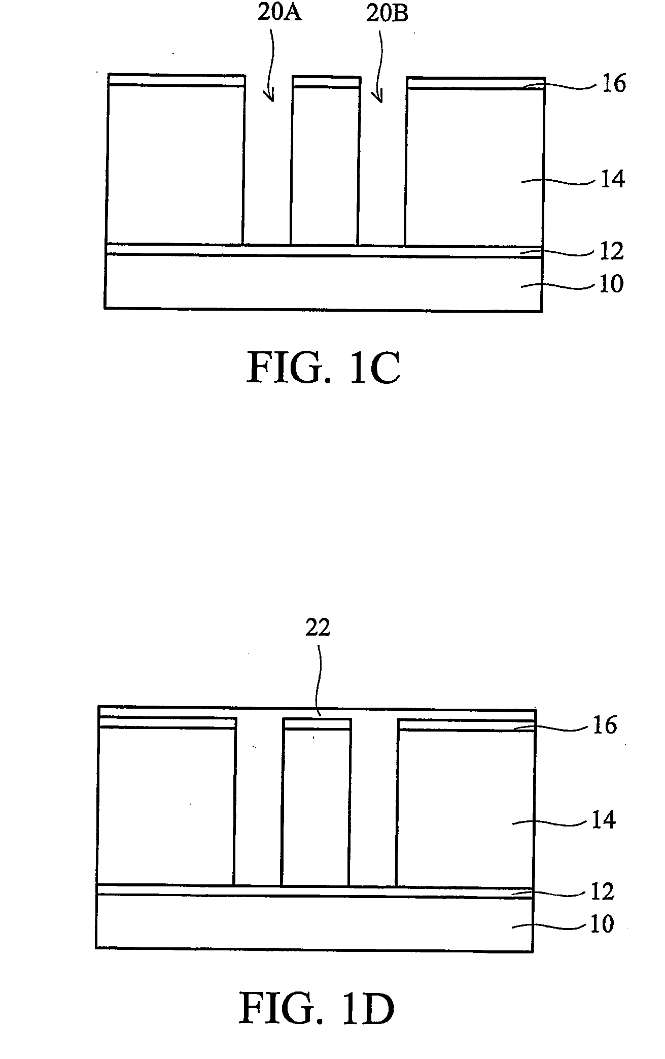
[0015] Although the method of the present invention is particularly advantageous for forming dual damascenes for wiring integrated circuits with characteristic dimensions less than about 0.13 microns including 65 nm and below, e.g., having a via diameter of about 0.12 microns or less, it will be appreciated that the method of the present invention may be applied to larger characteristic dimensioned integrated circuits and via diameters. The method of the present invention is particularly advantageous in reliably preventing damage to via sidewalls, avoiding the problems of photoresist and via poisoning, and reducing a number of processing steps to improve a process flow.
[0016] It will further be appreciated that the method may be applicable to dual damascenes with or without middle etch stop layers formed between dielectric insulating layers (i.e. IMD) to separate a via portion and trench portion of the dual damascene, although a middle etch stop layer is less preferred due to an un...
PUM
| Property | Measurement | Unit |
|---|---|---|
| dielectric constant | aaaaa | aaaaa |
| temperature | aaaaa | aaaaa |
| diameter | aaaaa | aaaaa |
Abstract
Description
Claims
Application Information