
Thermoelectric module and manufacturing method for same

a technology of thermoelectric modules and manufacturing methods, applied in the field of thermoelectric modules, can solve the problems of shortened manufacturing times, increased number of processes, and reduced production yields

Inactive Publication Date: 2006-08-17
YAMAHA CORP
View PDF1 Cites 14 Cited by
  • Summary
  • Abstract
  • Description
  • Claims
  • Application Information

AI Technical Summary

Benefits of technology

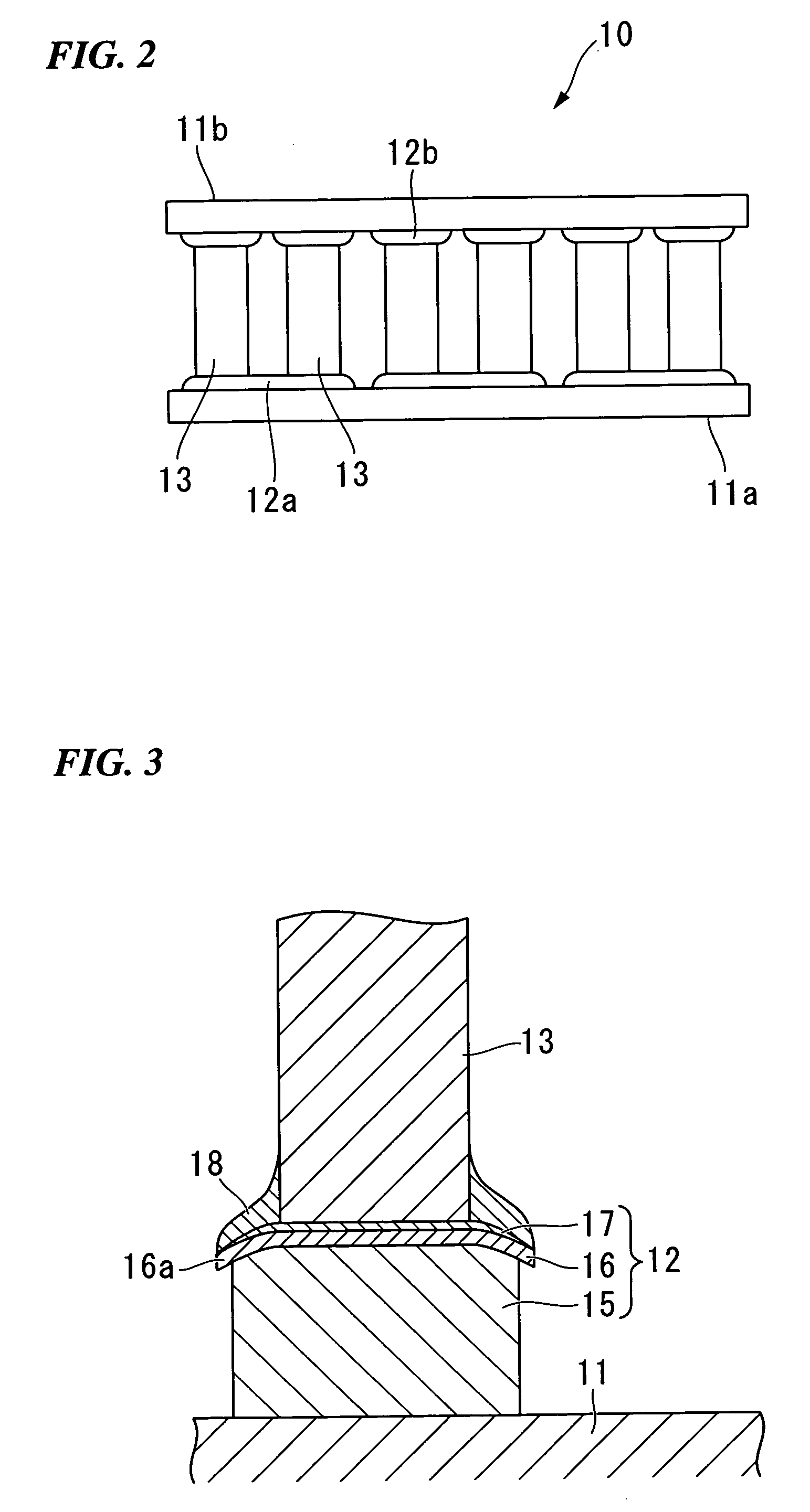
[0011] In order to attain this object, a thermoelectric module of this invention is configured by forming electrodes at prescribed locations on the opposing inside surfaces of a pair of insulating substrates, arranged in opposition, and by soldering the end faces of a plurality of thermoelectric elements to the respective opposing electrodes, to fix the thermoelectric elements between the pair of insulating substrates, and is characterized in that a visor portion, protruding outward, is formed on the edge portion of the thermoelectric element-side portion of the electrodes, and when thermoelectric elements are positioned on the upper sides of electrodes and electrodes soldered to thermoelectric elements, the solder is prevented from flowing from the side portions of the electrodes to the insulating substrates.
[0013] As a result, events in which the solder flows as far as the insulating substrate surface, making contact with solder which has flowed from other electrodes and causing short-circuits between electrodes, can be prevented. Further, when fixing the other end portions of thermoelectric elements to electrodes formed on the other insulating substrate also, with the insulating substrate positioned below, by fixing the lower end portions of the thermoelectric elements to the upper faces of electrodes positioned on the upper surface of the insulating substrate, flowing of solder to the insulating substrate can be prevented.
[0018] Because of its superior conductivity, copper is widely used in electrodes, and because of its superior solderability with respect to solder, gold is appropriate as the surface layer of electrodes when an electrode is to be fixed to a thermoelectric element by means of solder. And by forming a layer of nickel, with less solderability with respect to solder, between the copper layer and the gold layer, causing the edge portion of the nickel layer to protrude so as to form a visor portion, flowing of molten-state solder to the side of the insulating substrate can be reliably-prevented. In this case, the peripheral portion of the gold layer may be formed to protrude toward the outside together with the nickel layer visor portion; however, the side portion of the visor portion must be exposed without being covered.
[0019] Still another configuration characteristics of a thermoelectric module of this invention is the configuration of electrodes from a single layer consisting of a metal layer of one type. In this case the metal used in the metal layer is required to have superior conductivity and also to have less solderability with respect to solder, and so it is appropriate that nickel or magnesium be used. By this means, although the strength of adhesion of electrodes and thermoelectric elements due to the solder is somewhat weaker, the reliability with which short-circuits between electrodes due to solder can be prevented is increased. Further, because the number of processes for forming electrodes is reduced, thermoelectric modules can be easily manufactured, and costs can be reduced. Still another configuration characteristics of a thermoelectric module of this invention is the setting of both the thickness of the base end and protrusion length of the visor portion to 1 μm or greater. Here, the base end of the visor portion is the border portion between the main portion of the electrode and the visor portion. By this means, when soldering electrodes and thermoelectric elements, the visor portion can be ensured to be sufficiently strong and long enough to prevent the flow of molten solder.
[0021] By this means, a simple method can be used to obtain a thermoelectric module in which the flowing of solder to the insulating substrates is prevented, and short-circuits between electrodes due to solder do not occur. The resist layer formed in the resist layer formation process is not limited to direct formation on one surface of the insulating substrates, but may be formed via a prescribed seed layer. When forming a seed layer, this seed layer is removed by ion beam etching after removal of the resist layer.
[0024] By this means, a simple method can be used to obtain a thermoelectric module in which the flowing of solder to the insulating substrates is prevented, and short-circuits between electrodes due to solder do not occur. In this case, electrodes formed in the electrode formation process may be configured from single layers consisting of a single type of metal layer, or may be configured from a multilayer film consisting of a plurality of metal layers.

Problems solved by technology

However, of the above-described thermoelectric modules, the former entails the difficulty of processing to cause the nickel layer to be exposed on the side faces of the electrodes, as a result of which there are the problems that the number of processes is increased, production yields are lowered and manufacturing times lengthened, and in addition costs are increased.
In methods to manufacture such thermoelectric modules, prior to removal by-etching of the unwanted portions of the metal plated layer (the side-face portions of the electrodes), resist is formed on the upper surface of the metal plated layer; and there is the problem that during this processing, a shift in the electrodes and mask causes resist to touch the side faces of electrodes, giving rise to short-circuits.
Further, in the case of the latter thermoelectric modules of the prior art, grooves are formed between the electrodes on the insulating substrates respectively, so that the distances between electrodes are increased, and there is the problem that the thermoelectric modules are increased in size (with reduced densities).
Moreover, because grooves are formed, the number of processes is increased, production yields are lowered and manufacturing time is prolonged as well as increased costs.

Method used


Image

  • Thermoelectric module and manufacturing method for same
  • Thermoelectric module and manufacturing method for same
  • Thermoelectric module and manufacturing method for same

Examples


Embodiment Construction

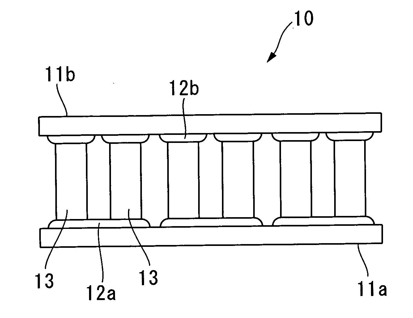
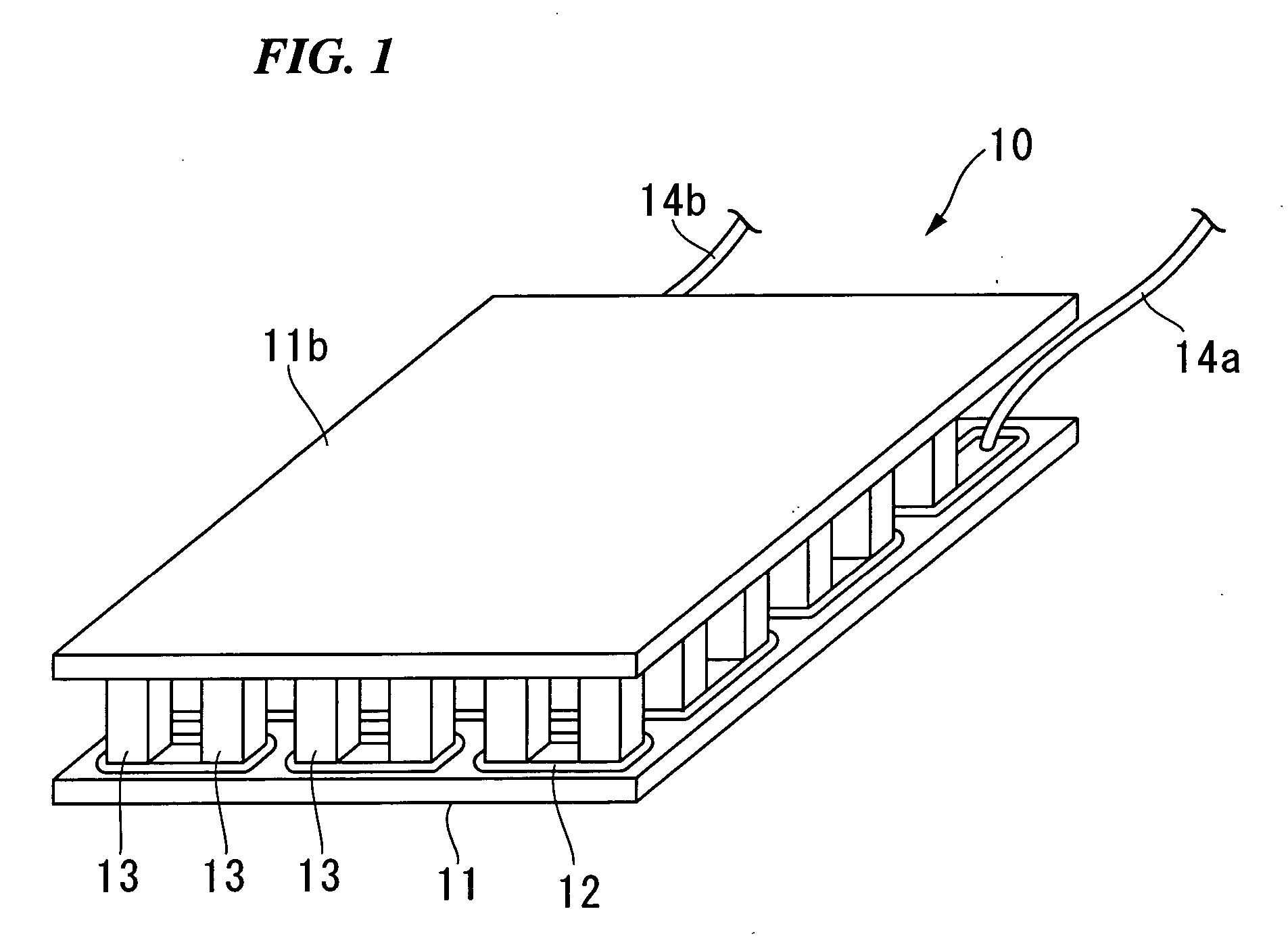
[0035] Hereinafter, embodiments of the present invention are explained referring to the drawings. FIG. 1 and FIG. 2 show a thermoelectric module 10 of one embodiment. This thermoelectric module 10 has a pair of insulating substrates, which are a lower substrate 11a and an upper substrate 11b; lower electrodes 12a are formed in prescribed positions of the upper surface of the lower substrate 11a, and upper electrodes 12b are formed in prescribed positions of the lower surface of the upper substrate 11b. The lower-end faces of multiple thermoelectric elements 13, consisting of chips, are fixed in place to the lower electrodes 12a by solder; and, the upper-end faces are fixed with solder to the upper electrodes 12b respectively, to integrally link the lower substrate 11a and the upper substrate 11b.

[0036] The lower electrodes 12a and upper electrodes 12b are installed at positions shifted distances equal to substantially the width of one of the thermoelectric elements 13. Upper electr...


PUM

PropertyMeasurementUnit
Lengthaaaaaaaaaa
Thermoelectricityaaaaaaaaaa

Abstract

A thermoelectric module and method of manufacture thereof, capable of preventing short-circuits between electrodes due to solder without causing increases in size or cost. A thermoelectric module is configured with lower electrodes formed on the inside surface of a lower substrate, placed in opposition to an upper substrate, on the inside surface of which are formed upper electrodes; the end faces of thermoelectric elements are soldered to the lower electrodes and upper electrodes. Each of the electrodes is configured from three layers, which are a copper layer, a nickel layer formed on one face of the copper layer, and a gold layer formed on one face of the nickel layer; a visor portion, protruding outward, is formed in the nickel layer, so that when positioning the thermoelectric elements above the electrodes and soldering the electrodes to the thermoelectric elements, the flowing of solder 18a from the side portions of electrodes to the insulating substrate is prevented.

Description

BACKGROUND OF THE INVENTION [0001] 1. Field of the Invention [0002] This invention relates to a thermoelectric module which performs thermoelectric conversion, and to a manufacturing method for same. [0003] Priority is claimed on Japanese Patent Application No. 2005-37767, filed Feb. 15, 2005, the content of which is incorporated herein by reference. [0004] 2. Description of Related Art [0005] Thermoelectric modules, which utilize the Peltier effect and the Seebeck effect in thermoelectric power conversion, have conventionally been used in heating and cooling equipment and other applications. Such thermoelectric modules are configured by forming multiple electrodes at prescribed locations on the opposing inside surfaces of a pair of insulating substrates, and by soldering the upper and lower ends of thermoelectric elements to the opposing electrodes, to fix in place multiple thermoelectric elements between the pair of insulating substrates. [0006] Among such thermoelectric modules, ...

Claims


Application Information

Patent Timeline
IPC IPC(8): H01L37/00H01L35/34H01L35/30H01L35/28
CPCH01L35/08H10N10/817
Inventor YASUTAKE, HIDETOSHI
Owner YAMAHA CORP
Learn More