Wiring board manufacturing method

a manufacturing method and wiring board technology, applied in the direction of printed circuit aspects, printed circuit stress/warp reduction, conductive pattern formation, etc., can solve the problems of wiring board warpage, difficult to achieve difficult to realize the reduction of wiring board thickness and the higher density of wiring board, etc., to reduce the thickness of wiring board, reduce the warpage of such a wiring board, and facilitate the connection between the wiring and the semiconductor chip.

Active Publication Date: 2006-09-21
SHINKO ELECTRIC IND CO LTD
View PDF5 Cites 37 Cited by
  • Summary
  • Abstract
  • Description
  • Claims
  • Application Information

AI Technical Summary

Benefits of technology

[0021] In the method of manufacturing the wiring board according to the invention, reliability of connection between the wiring and the semiconductor chip becomes favorable.
[0022] According to the invention, the reduction in the thickness of the wiring board incorporating semiconductor chips is achieved, and the suppression of the warpage of such a wiring board is possible.

Problems solved by technology

However, in a case where reduction in thickness (thin) and higher-density in the built-in chip type wiring board are realized, warpage of the wiring board may be a problem.
Consequently, in the built-in chip type wiring board with such a laminated structure, it is difficult to realize the reduction in the thickness of the wiring board and the higher-density in the wiring board.
Also, it is difficult to achieve the reduction in the thickness of the wiring board while suppressing the warpage of the wiring board.

Method used


Image

  • Wiring board manufacturing method
  • Wiring board manufacturing method
  • Wiring board manufacturing method

Examples


first embodiment

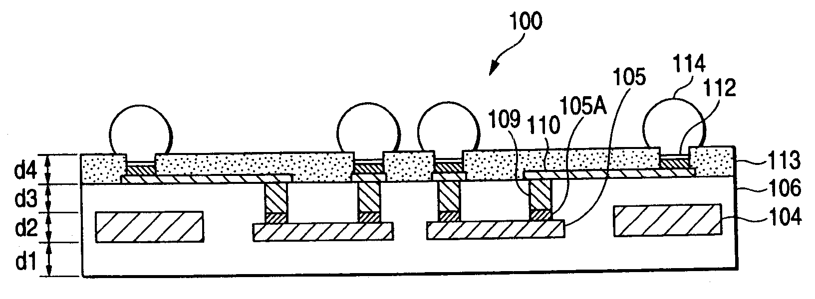
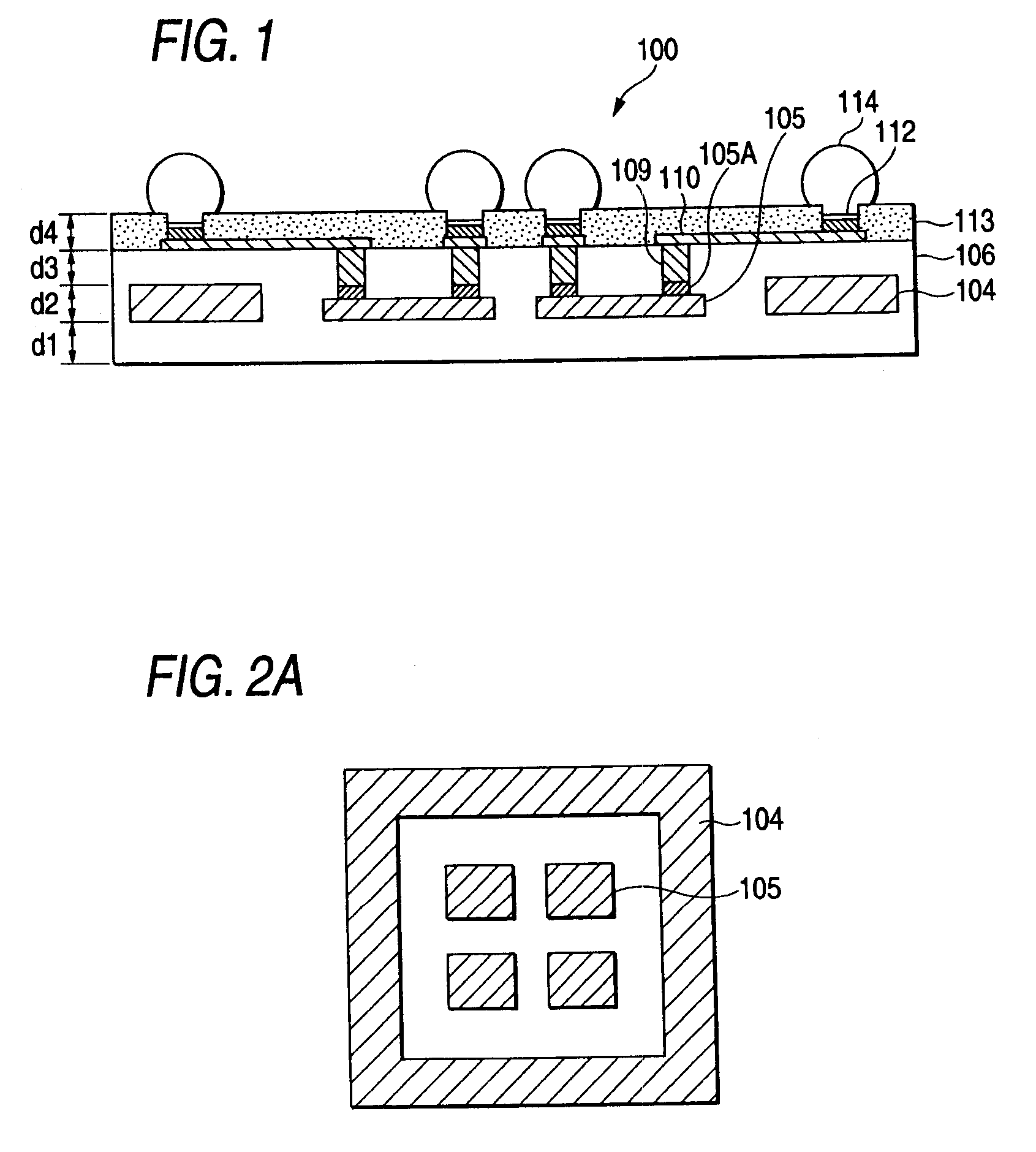
[0054]FIG. 1 is a cross-sectional view schematically showing a wiring board according to a first embodiment of the invention. Referring to FIG. 1, a wiring board 100 shown in this figure has an insulating layer 106 made of, for example, an epoxy resin or a polyimide resin. The wiring board 100 has a structure in which at least one semiconductor chip 105 is embedded in the insulating layer 106.

[0055] A bump 105A made of, for instance, NiP (nickel-phosphorus) is formed on an electrode pad (not shown) of the semiconductor chip 105. A via plug 109 made of, for instance, Cu is formed on the bump 105A so as to be erected thereon. Also, a pattern wiring 110 made of, for example, Cu is formed on the insulating layer 106 integrally with the via plug 109 so as to be connected to the via plug 109.

[0056] Also, a terminal connection portion 112 including, for example, a Ni / Au layer is formed on the pattern wiring 110. A solder resist layer 113 is formed on the pattern wiring 110 and the insula...

second embodiment

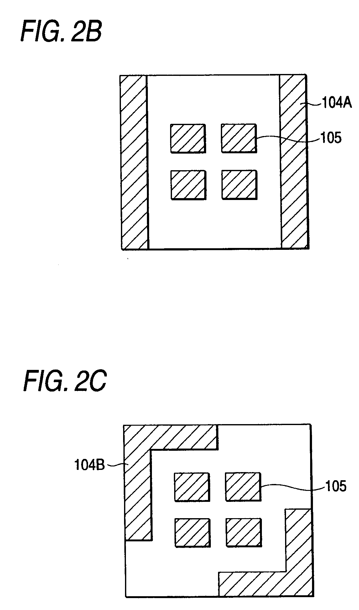
[0095] The wiring board according to the invention is not limited to that according to the first embodiment. Various modifications and alterations of, for example, the wiring structure or the reinforcing member may be made.

[0096] For example, FIG. 4 shows a wiring board 200 according to a second embodiment of the invention.

[0097] Referring to FIG. 4, in the wiring board 200 shown in this figure, an insulating layer 206, a reinforcing member 204, a semiconductor chip 205, a pattern wiring 210, a terminal connection portion 212, a solder resist layer 213, and a solder ball 214 respectively correspond to the insulating layer 106, the reinforcing member 104, the semiconductor chip 105, the pattern wiring 110, the terminal connection portion 112, the solder resist layer 113, and the solder ball 114 shown in the wiring board 100 shown in FIG. 1. These structures of the wiring board 200 are similar to those of the wiring board 100.

[0098] In the wiring board 200 according to this embodim...


PUM

PropertyMeasurementUnit
distance d1aaaaaaaaaa
thickness d2aaaaaaaaaa
distance d3aaaaaaaaaa

Abstract

A method of manufacturing a wiring board includes: forming a first insulating layer on a supporting board; mounting at least one reinforcing member on the first insulating layer; mounting at least one semiconductor chip on the first insulating layer; forming a second insulating layer on the reinforcing member and the semiconductor chip; and forming a wiring on the second insulating layer, the wiring being connected to the semiconductor chip.

Description

[0001] This application claims foreign priority based on Japanese Patent application No. 2005-073945, filed Mar. 15, 2005, the content of which is incorporated herein by reference in its entirety. BACKGROUND OF THE INVENTION [0002] 1. Field of the Invention [0003] The present invention relates to a method of manufacturing a wiring board, and more particularly, to a method of manufacturing a wiring board incorporating a semiconductor chip. [0004] 2. Description of the Related Art [0005] Currently, enhancement in performance of electronic devices using semiconductor devices such as semiconductor chips has been advanced. Higher-density of semiconductor chips mounted on a board, reduction in size of the board on which the semiconductor chips are mounted, and saving of space in the board are demanded. [0006] Thus, a board in which a semiconductor chip is embedded, that is, a built-in chip type wiring board has been proposed. Various configurations for incorporating the semiconductor chip...

Claims


Application Information

Patent Timeline
Patent Type & Authority Applications(United States)
IPC IPC(8): H05K3/36
CPCH01L21/6835Y10T29/49165H01L23/5386H01L23/5389H01L24/18H01L24/82H01L25/0655H01L2221/68345H01L2224/18H01L2224/82039H01L2924/01015H01L2924/01029H01L2924/01033H01L2924/01078H01L2924/01079H01L2924/01082H01L2924/15311H05K1/0271H05K1/185H05K3/007H05K2201/2009H05K2203/016H01L2924/01006H01L2924/01019H01L2924/01023H01L2924/014Y10T29/49126Y10T29/4913Y10T29/49128Y10T29/49144Y10T29/49155H01L23/49816H01L21/568H01L2224/04105H01L2224/12105H01L2924/181H01L2924/3511H01L24/19H01L24/24H01L2924/00H01L25/04H01L23/12
Inventor YAMANO, TAKAHARU
Owner SHINKO ELECTRIC IND CO LTD
Why Eureka
Try Eureka