Porous processing carrier for flexible substrates

a flexible substrate and processing carrier technology, applied in the field of glass substrates, can solve the problems of increasing the weight of the larger display, affecting the production efficiency of fusion glass thinners, and affecting the ability of tft manufacturing technology to accommodate fusion glass thinners

Inactive Publication Date: 2006-09-21
CORNING INC
View PDF19 Cites 60 Cited by
  • Summary
  • Abstract
  • Description
  • Claims
  • Application Information

AI Technical Summary

Benefits of technology

[0012] In one embodiment according to the present invention, a substrate product for use in the manufacture of an electronic device is provided comprising a porous support substrate an adhesive layer disposed on the support substrate a display s

Problems solved by technology

However, this raises several issues.
First, the increased weight of the larger display is problematic.
Unfortunately, if the thickness of the glass is decreased, the elastic sag of the glass substrate becomes a problem.
Presently, it is difficult for TFT manufacturing technology to accommodate fusion glass thinner that 0.5 mm because of glass sag.
Thinner, larger substrates have a negative impact on the processing robotics' ability to load, retrieve, and s

Method used


Image

  • Porous processing carrier for flexible substrates
  • Porous processing carrier for flexible substrates
  • Porous processing carrier for flexible substrates

Examples


Embodiment Construction

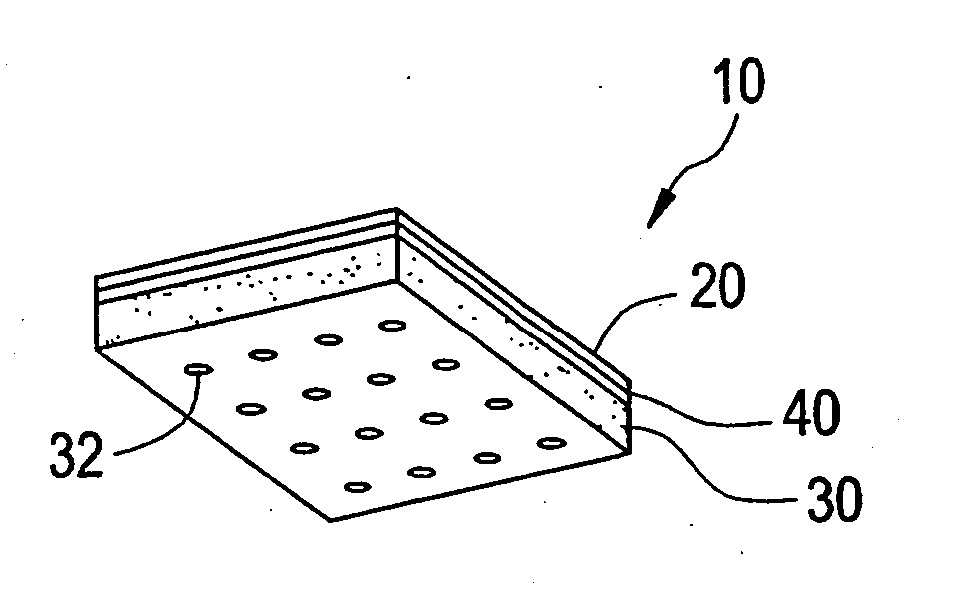
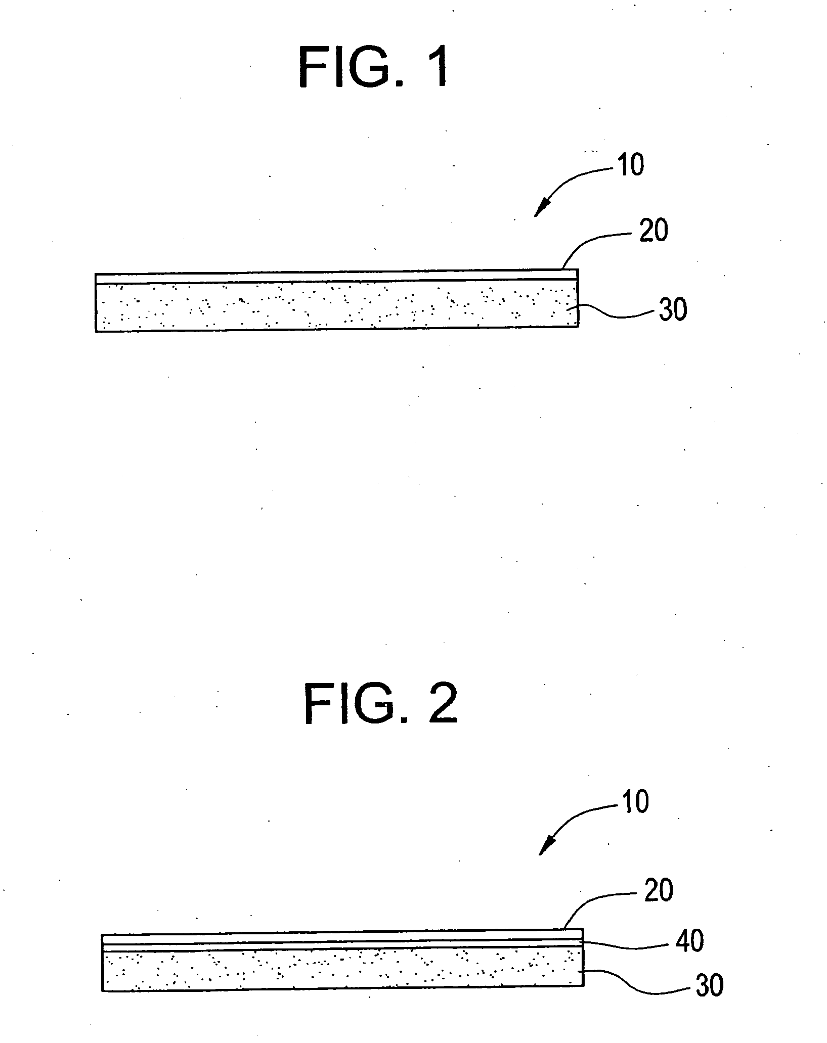
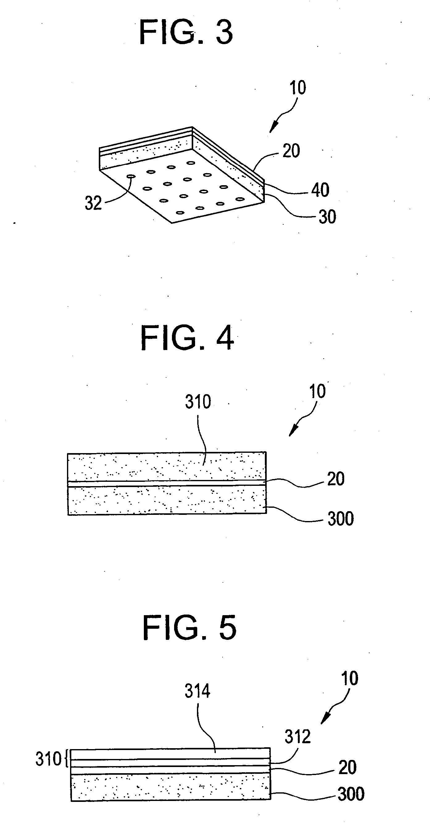
[0026] Reference will now be made in detail to the present exemplary embodiments of the invention, examples of which are illustrated in the accompanying drawings. Wherever possible, the same reference numbers will be used throughout the drawings to refer to the same or like parts. An exemplary embodiment of the substrate product of the present invention is shown in FIG. 1, and is designated generally throughout by reference numeral 10.

[0027] In accordance with the invention, the present invention is directed to a substrate product for use in the manufacture of flexible electronic panels. Flexible electronic panels can encompass such electronic products as radio frequency identification tags (RFIDs), photovoltaics (e.g. solar cells), printable electronics, as well as other flexible products. The substrate product disclosed herein is especially suitable for the manufacture of active matrix liquid crystal displays (AMLCD), organic light emitting diode displays (OLEDs), electrophoretic...


PUM

PropertyMeasurementUnit
Thicknessaaaaaaaaaa
Diameteraaaaaaaaaa
Pressureaaaaaaaaaa

Abstract

The present invention is directed to a substrate product for use in the manufacture of active matrix liquid crystal display panels, flexible displays, or flexible electronics. The product includes a display substrate suitable for use as a display panel. The display substrate has a thickness less than or equal to 0.4 mm. The product also includes at least one porous support substrate removably attached to the display substrate by an adhesive layer.

Description

[0001] This is a continuation-in-part of U.S. patent application Ser. No. 10 / 613,972 filed on Jul. 3, 2003, the content of which is relied upon and incorporated herein by reference in its entirety, and the benefit of priority under 35 U.S.C. § 120 is hereby claimed.BACKGROUND OF THE INVENTION [0002] 1. Field of the Invention [0003] The present invention relates generally to glass substrates suitable for use in flexible electronic devices, and is particularly beneficial to a glass substrate product for use in AMLCD, OLED, and flexible display manufacturing processes. [0004] 2. Technical Background [0005] Liquid crystal displays (LCDs) are non-emissive displays that use external light sources. An LCD is a device that may be configured to modulate an incident polarized light beam emitted from the external source. LC material within the LCD modulates light by optically rotating the incident polarized light. The degree of rotation corresponds to the mechanical orientation of individual L...

Claims


Application Information

Patent Timeline
IPC IPC(8): B29D11/00B44C1/22B32B3/10B32B7/06B32B17/06C03C19/00C03C27/10C09K19/52G02FG02F1/1333G02F1/136G02F1/1362
CPCB32B7/06Y10T428/24273C03C19/00C03C27/10C03C2218/355G02F1/1333G02F2001/133302G02F2001/13613G02F2001/136295H01L21/6835H01L2221/68318H01L2221/6835H01L2221/68381B32B7/14B32B9/005B32B3/266B32B2457/20B32B2457/206B32B17/06G02F1/133302G02F1/13613G02F1/136295B29D11/00B44C1/22B32B3/10
Inventor BOCKO, PETER LAWRENCEGARNER, SEAN MATTHEWGILLBERG, GUNILLA ELSALAPP, JOSEF CHAUNCEY
Owner CORNING INC
Why Eureka
Try Eureka