Nitride micro light emitting diode with high brightness and method of manufacturing the same

Inactive Publication Date: 2006-09-21
KANG DA
View PDF2 Cites 71 Cited by
  • Summary
  • Abstract
  • Description
  • Claims
  • Application Information

AI Technical Summary

Benefits of technology

[0036] According to the present invention as described above, by filling gaps between the luminous pillars in the nitride micro luminous pillar array with the gap filling material, planarizing the resultant structure using the CMP process, and forming the transparent electrode on the surface thereof, it is possible to maximize the luminous area and thus to externally use the light emitted from the active layer with a high efficiency.
[0037] In addition, it is possible to provide the nitride micro LED with high brightness, which consumes the same power as the conventional large-area LED and of which the luminous efficiency is more excellent.
[0038] Further, according to the present invention, by using the nitride micro LED with high brightness having an improv

Problems solved by technology

Since most GaN is grown using a heterogeneous epitaxy technology, a plurality of lattice defects necessarily exist therein, thereby resulting in deterioration of the internal luminous efficiency.
Nonethe

Method used


Image

  • Nitride micro light emitting diode with high brightness and method of manufacturing the same
  • Nitride micro light emitting diode with high brightness and method of manufacturing the same
  • Nitride micro light emitting diode with high brightness and method of manufacturing the same

Examples


first embodiment

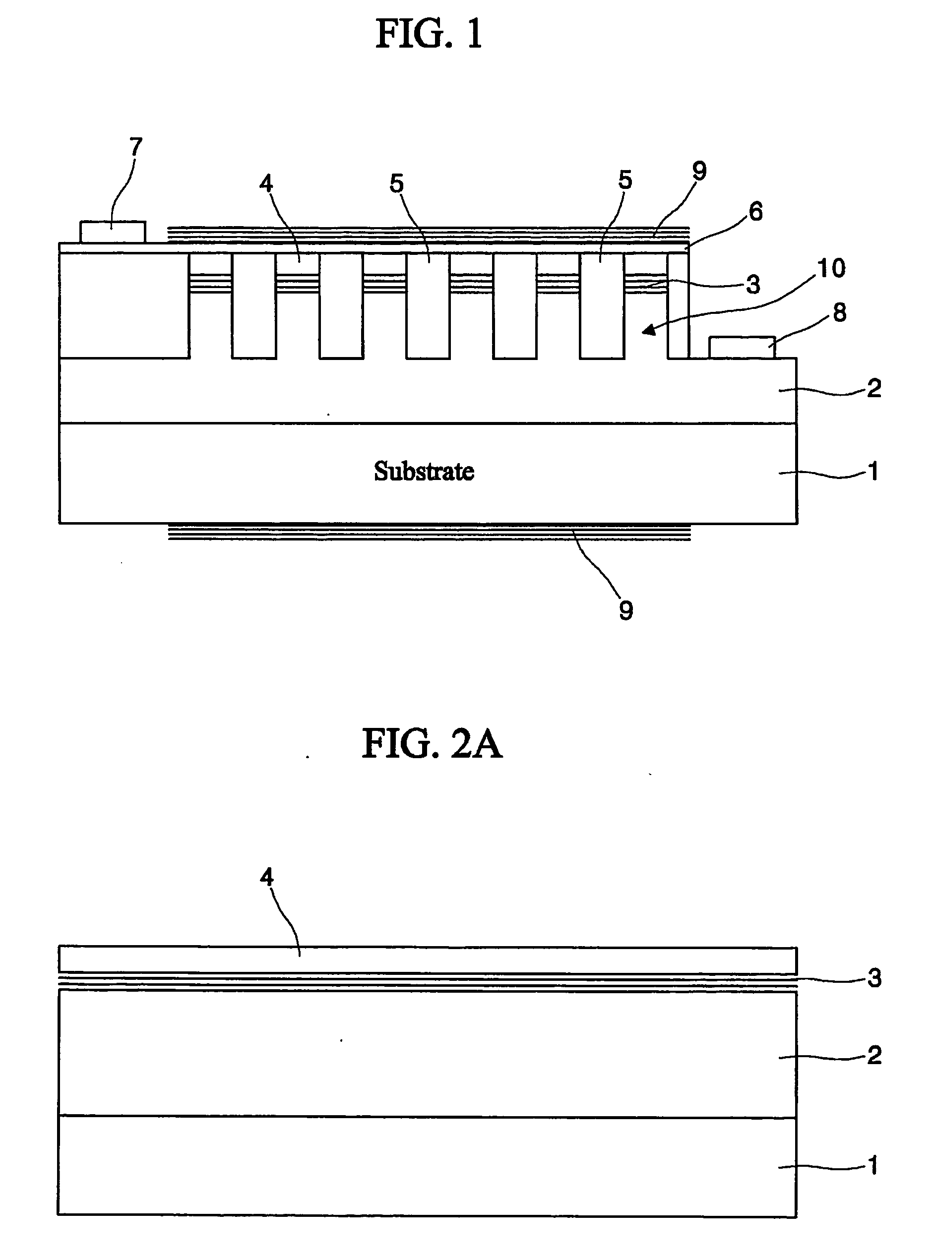
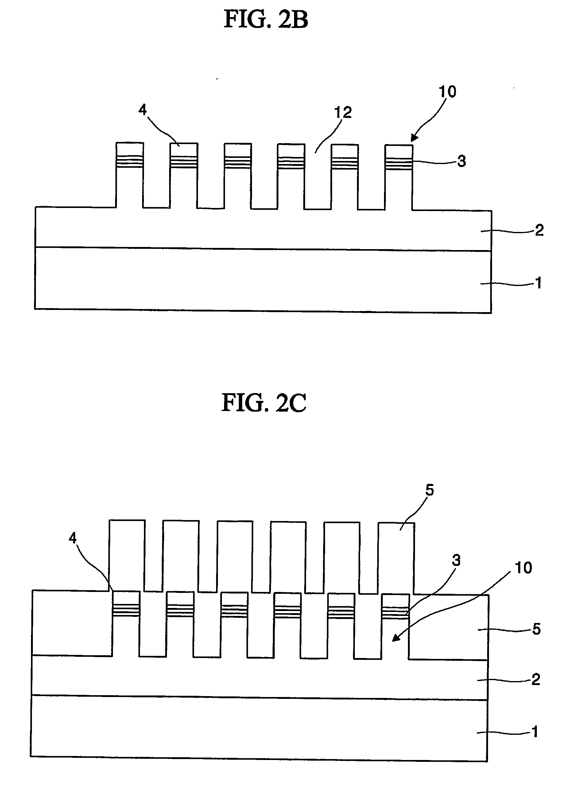
[0041]FIG. 1 is a view illustrating a micro LED according to one embodiment of the present invention, and FIGS. 2A to 2E are views illustrating a method of manufacturing the micro LED shown in FIG. 1.

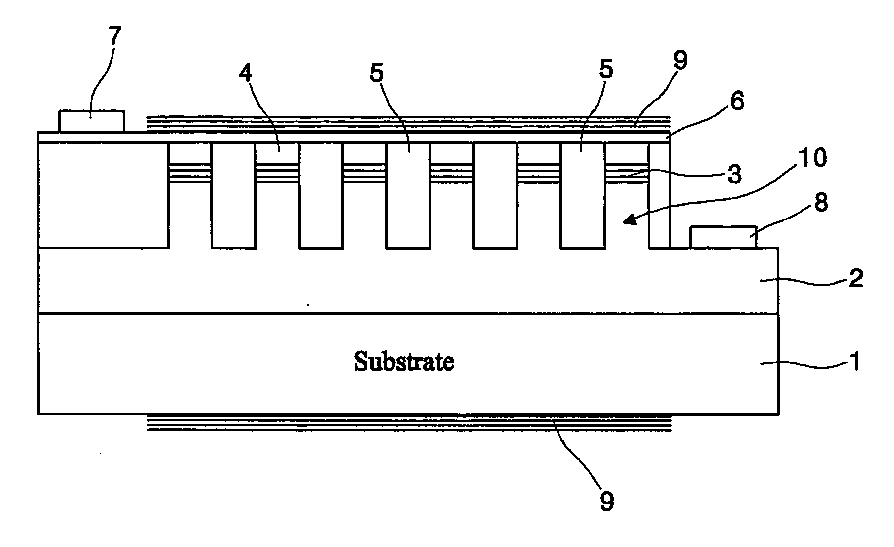
[0042] As shown in FIG. 1, a nitride micro LED with high brightness according to the present invention comprises a substrate 1, a n-type GaN layer 2, an active layer 3, a p-type GaN layer 4, a gap filling material 5, a transparent electrode 6, a p-type electrode 7, an n-type electrode, and a DBR (Distributed Bragg Reflectors) layer 9. The reference numeral 10 in FIG. 1 denotes micro-sized luminous pillars.

[0043] Specifically, the n-type GaN layer 2, the InGaN / GaN active layer 3, the p-type GaN layer 4 sequentially grown and disposed on the sapphire (Al2O3) substrate 1 grown in a predetermined direction constitutes a plurality of micro-sized luminous pillars or luminous element pillars 10.

[0044] The luminous element pillars 10 are formed to be a circular cylinder shape in order to max...

second embodiment

[0069]FIGS. 6A to 6D are views illustrating a method of manufacturing the micro LED using a selective re-growth method in place of a dry etching method in manufacturing the micro LED in the first embodiment.

[0070] The second embodiment employs a selective re-growth method, unlike the first embodiment employing the dry etching method for formation of the luminous pillars 10. In this case, the second embodiment does not require the CMP process.

[0071] As shown in FIG. 6A, first, a GaN buffer layer 2a for re-growing the luminous pillars 10 (see FIG. 6D) is grown on the substrate 1, and then the oxide film 5 is deposited thereon in a thickness of the luminous pillars desired to obtain. By patterning the oxide film 5 using a wet etching method, the shape shown in Fig. B is obtained, and the re-growth is carried out using the exposed GaN buffer layer 2a (see FIG. 6C). As the re-grown layer, the n-type GaN layer 2, the InGaN / GaN QW active layer 3 and the p-type GaN layer 4 are grown on th...


PUM


Abstract

The present invention relates to a nitride micro light emitting diode (LED) with high brightness and a method of manufacturing the same. The present invention provides a nitride micro LED with high brightness and a method of manufacturing the same, wherein a plurality of micro-sized luminous pillars 10 are formed in a substrates, a gap filling material such as SiO2, Si3N4, DBR(ZrO2/SiO2 HfO2/SiO2), polyamide or the like is filled in gaps between the micro-sized luminous pillars, a top surface 11 of the luminous pillar array and the gap filling material is planarized through a CMP processing, and then a transparent electrode 6 having a large area is formed thereon, so that all the luminous pillars can be driven at the same time. In addition, the present invention provides a nitride micro LED with high brightness in which uniformity in formation of electrodes on the micro-sized luminous pillars array is enhanced by employing a flip-chip structure.

Description

FIELD OF THE INVENTION [0001] The present invention relates to a nitride micro light emitting diode (LED) with high brightness and a method of manufacturing the same, and specifically to a nitride micro light emitting diode (LED) with high brightness and a method of manufacturing the same, in which luminous efficiency is maximized by finely adjusting micro-sized nitride luminous elements and allowing an array of the elements to be driven at the same time. BACKGROUND OF THE INVENTION [0002] In recent, because of excellent characteristics of a gallium nitride (GaN) semiconductor, a nitride semiconductor LED is widely studied. [0003] Specifically, in order to use the nitride LED for illumination as well as for display, the brightness limit of the commercialized LED should be overcome. [0004] The nitride LED generally emits light in an element area having a diameter of 300 μm or more. The light emitted from a luminous layer may not get out of the element and be locked in the element, so...

Claims


Application Information

Patent Timeline
IPC IPC(8): H01L33/00H01L21/30H01L33/06H01L33/08H01L33/10H01L33/12H01L33/32H01L33/42H01L33/44
CPCH01L33/08H01L33/32H01L33/42H01L33/44
Inventor KANG
Owner KANG DA
Why Eureka
Try Eureka