Wiring board and method of manufacturing the same

a manufacturing method and technology of wiring board, applied in the direction of printed circuit manufacturing, printed circuit non-printed electric components association, conductive pattern formation, etc., can solve the problems of warpage difficult to realize the higher density difficulty in achieving the reduction of the thickness of the wiring board. , to achieve the effect of reducing the thickness of the wiring board, stably forming, and high density of the wiring structur

Inactive Publication Date: 2006-09-21
SHINKO ELECTRIC IND CO LTD
View PDF13 Cites 88 Cited by
  • Summary
  • Abstract
  • Description
  • Claims
  • Application Information

AI Technical Summary

Benefits of technology

[0023] The method of manufacturing the wiring board of the invention further comprises: forming a via plug in the insulating layer, and connecting the via plug to the lower-layer wiring structure; and forming an upper-layer wiring structure so that the semiconductor chip is mounted between the lower-layer wiring structure and the upper-layer wiring structure, and connecting the upper-layer wiring structure to the via plug. Thus, a higher-density of the wiring structure can be achieved. Consequently, this embodiment is favorable.
[0024] In the method of manufacturing the wiring board of the invention, the lower-layer wiring structure is formed on a core board, and the method further comprises: removing the core board. Thus, reduction in the thickness of the wiring board can be achieved. Also, the wiring board can stably be formed. Consequently, this embodiment is favorable.
[0025] In the method of manufacturing the wiring board of the invention, the core board is made of an electrically conductive material, and the forming step of the lower-layer wiring ...

Problems solved by technology

However, in a case where reduction in thickness (thin) and higher-density in the built-in chip type wiring board are realized, warpage of the wiring board may be a problem.
Consequently, in the built-in chip type wiring board with such a laminated struct...

Method used


Image

  • Wiring board and method of manufacturing the same
  • Wiring board and method of manufacturing the same
  • Wiring board and method of manufacturing the same

Examples


first embodiment

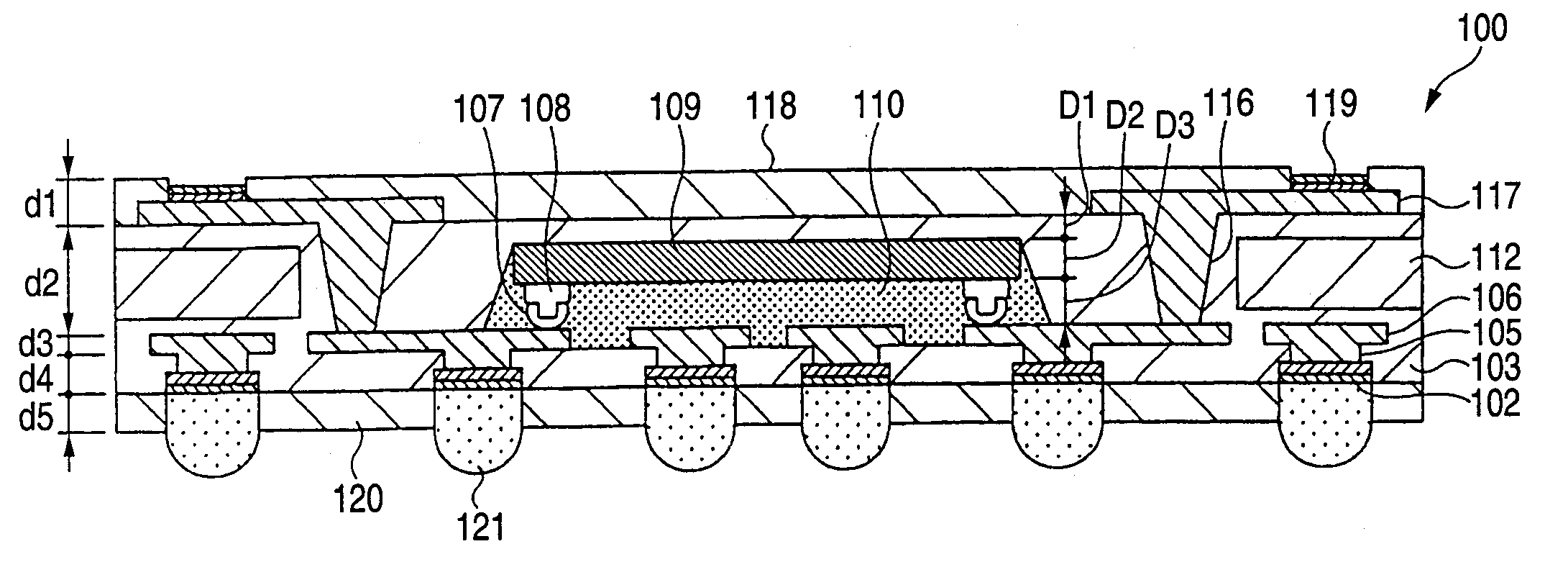
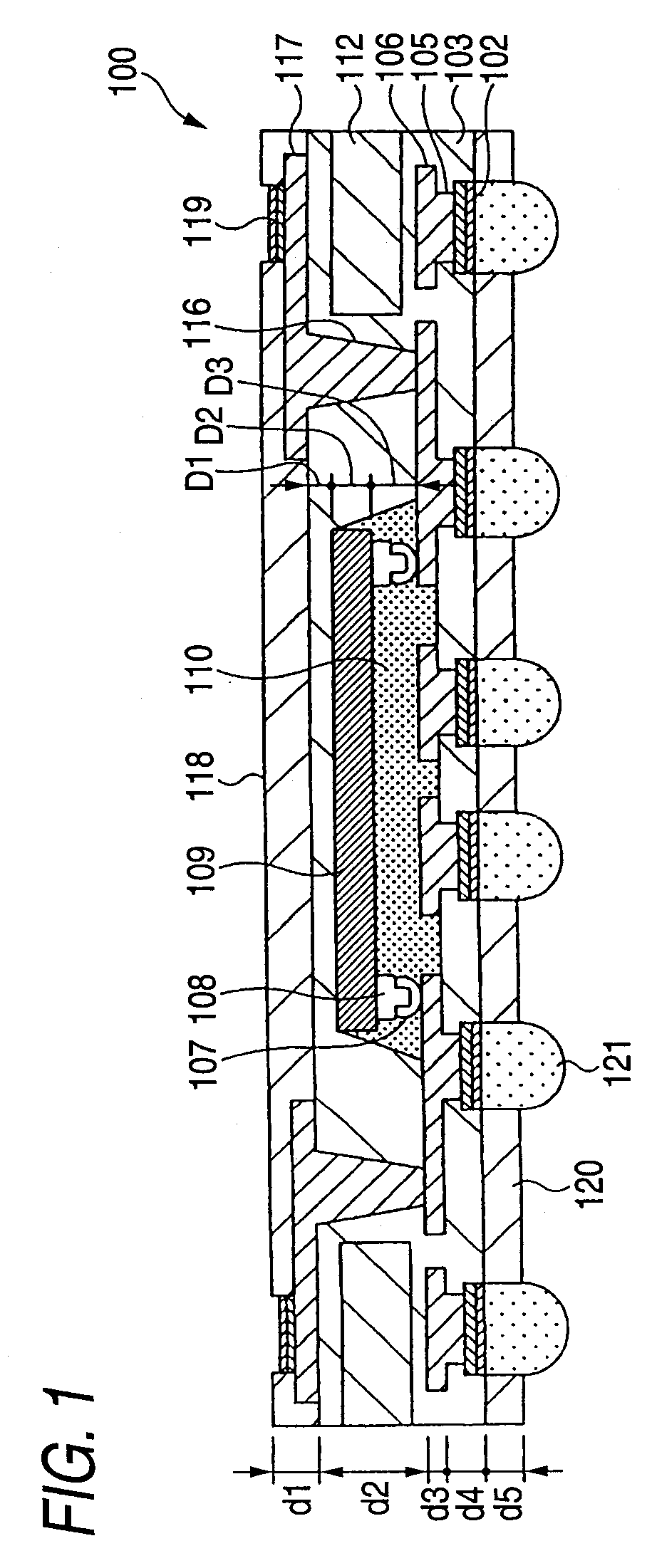
[0051]FIG. 1 is a cross-sectional view schematically showing a wiring board 100 according to a first embodiment of the invention.

[0052] Referring to FIG. 1, the wiring board 100 according to this embodiment includes a semiconductor chip 109 embedded in an insulating layer 103, and a wiring structure connected to the semiconductor chip 109. This wiring structure has pattern wirings 106 and 117, and via plugs 105 and 116.

[0053] Moreover, the wiring board 100 has a terminal connection portion 102 formed at a first side thereof and a terminal connection portion 119 formed at a second side which is opposite to the first side thereof. The terminal connection portions 102 and 119 are connected to the semiconductor chip 109 through the wiring structure.

[0054] Hitherto, in the case of reducing the thickness of such a built-in semiconductor chip type wiring board, the wiring board and a structural body such as a core board which supports the wiring board and suppresses the warpage of the w...


PUM

PropertyMeasurementUnit
Electrical conductivityaaaaaaaaaa
aaaaaaaaaa

Abstract

A wiring board includes an insulating layer in which a semiconductor chip is embedded, and a wiring structure connected to the semiconductor chip. A reinforcing member reinforcing the insulating layer is embedded in the insulating layer. This enables reduction in a thickness of the wiring board and a suppression of warpage of the wiring board.

Description

[0001] This application claims foreign priority based on Japanese Patent application No. 2005-073946, filed Mar. 15, 2005, the content of which is incorporated herein by reference in its entirety. BACKGROUND OF THE INVENTION [0002] 1. Field of the Invention [0003] The present invention relates to a method of manufacturing a wiring board, and more particularly, to a method of manufacturing a wiring board incorporating a semiconductor chip. [0004] 2. Description of the Related Art [0005] Currently, enhancement in performance of electronic devices using semiconductor devices such as semiconductor chips has been advanced. Higher-density of semiconductor chips mounted on a board, reduction in size of the board on which the semiconductor chips are mounted, and saving of space in the board are demanded. [0006] Thus, a board in which a semiconductor chip is embedded, that is, a built-in chip type wiring board has been proposed. Various configurations for incorporating the semiconductor chip...

Claims


Application Information

Patent Timeline
IPC IPC(8): H01L23/48
CPCH01L21/563H01L21/6835H01L23/18H01L23/3128H01L23/49805H01L23/49816H01L23/5383H01L23/5389H01L24/81H01L2221/68345H01L2224/1134H01L2224/13144H01L2224/16225H01L2224/73204H01L2224/8121H01L2224/81815H01L2224/83102H01L2224/92125H01L2924/01013H01L2924/01029H01L2924/01033H01L2924/01078H01L2924/01079H01L2924/01082H01L2924/15311H01L2924/15331H05K1/185H05K3/4644H01L2924/00013H01L2924/01006H01L2924/01019H01L2924/0105H01L2924/014H01L25/0655H01L2224/136H01L2224/32225H01L2924/3511H01L2224/81191Y10T29/49126Y10T29/49155Y10T29/4913Y10T29/49135Y10T29/49156H01L2924/00014H01L2224/13099H01L2924/00H01L2224/81005H01L2924/00011H01L2924/12042H01L2924/15192H01L2924/381H01L2224/0401H05K1/18H05K3/22
Inventor YAMANO, TAKAHARUSUNOHARA, MASAHIROIIZUKA, HAJIMEKOYAMA, TETSUYA
Owner SHINKO ELECTRIC IND CO LTD
Why Eureka
Try Eureka