LED device with flip chip structure

a technology of flip chip and diode, which is applied in the direction of semiconductor devices, semiconductor/solid-state device details, electrical apparatus, etc., can solve the problems of low productivity, waste of bonding wire space, and poor packaging structure for device miniaturization, etc., to increase the brightness of emitted light, low cost, and high productivity

Inactive Publication Date: 2006-09-21
LEDARTS OPTO
View PDF2 Cites 52 Cited by
  • Summary
  • Abstract
  • Description
  • Claims
  • Application Information

AI Technical Summary

Benefits of technology

[0011] A unique feature of the present invention is that the wire bonding process is eliminated in the manufacturing process. The room required for the wire bonding process is then saved. The thickness of the LED device of the present invention is more than 50% reduced as compared to a conventional LED device of same specification. Besides, the multiple reflective films in the LED flip chip significantly increase the brightness of emitted light. These films can also act as protection layers, which eliminate the need of a passive protection layer during the manufacturing process. Therefore, the LED device of the present invention has the advantages of low cost, high productivity, and suitability for device miniaturization.

Problems solved by technology

The above scheme not only lowers the productivity but also wastes a room required for the bonding wires.
This type of packaging structure is not good for device miniaturization.
This kind of manufacturing process is complicated and requires a long manufacturing time.
Moreover, the miniaturization capability of the LED device 200 is limited though it is still better than conventional LED devices.

Method used


Image

  • LED device with flip chip structure
  • LED device with flip chip structure
  • LED device with flip chip structure

Examples


Embodiment Construction

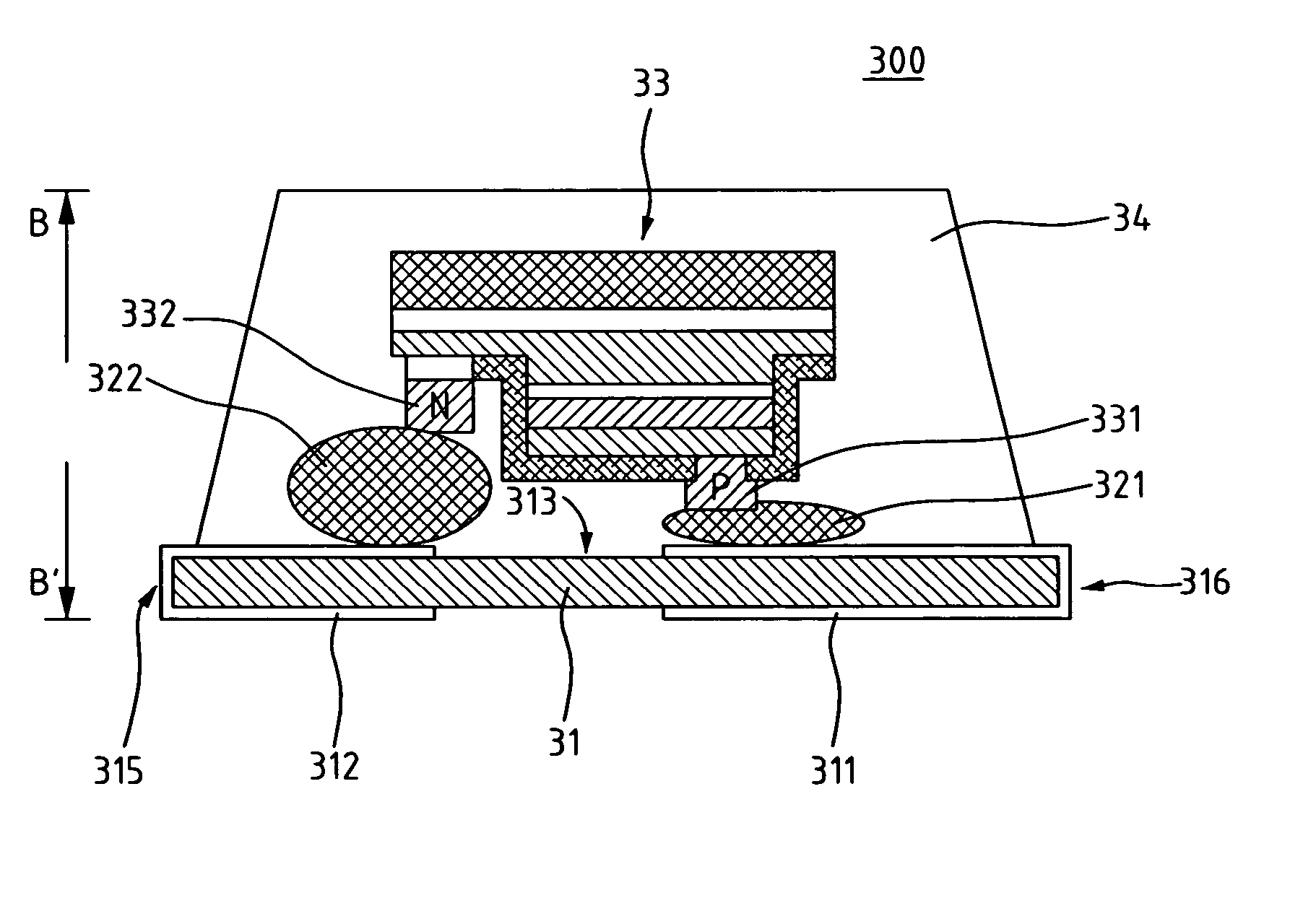
[0018]FIG. 3 depicts a cross-sectional view of a flip chip LED device of the present invention. As shown in FIG. 3, a flip chip LED device 300 comprises an insulating substrate 31, an LED flip chip 33, a molding compound 34, a first conductive element 321, and a second conductive element 322. The insulating substrate 31 has two side edges 315 and 316, a top surface 313, a down surface 314, a P-type electrode layer 311, and an N-type electrode layer 312. Every electrode layer is disposed near one side edge of the substrate 31 and extended to cover a portion of the top surface 313 and down surface 314 of the substrate 31. The P-type electrode layer 311 and the N-type electrode 312 can be used as connection pads to the outside electrical power.

[0019] The first conductive element 321 is located on the top of the P-type electrode layer 311. The second conductive element 322 is located on the top of the N-type electrode layer 312. The LED flip chip 33 having a P-type electrode 331 and an...


PUM


Abstract

The present invention provides an LED device with a flip chip structure. The LED device comprises an insulating substrate, an LED flip chip, a molding compound, a first conductive element, and a second conductive element. The LED flip chip is electrically connected to the connection pads on the insulating substrate via the two conductive elements. The P-type and N-type electrodes are connected to the P-type and N-type electrodes layers, respectively. The invention need not require a conventional wire bonding process. It not only increases the yield rate of the product but also makes the product more compact.

Description

FIELD OF THE INVENTION [0001] The present invention generally relates to a light emitting diode (LED) device, and more specifically to an LED device with a flip chip structure. BACKGROUND OF THE INVENTION [0002]FIG. 1 shows a cross-sectional structure of a conventional surface-mount device (SMD) type LED device. [0003] In a conventional SMD-type LED packaging structure, an LED die 13 is attached to a packaging substrate 11. The positive and negative electrodes of the LED die 13 are connected through gold or aluminum wires to a positive pad 111 and a negative pad 112 on the packaging substrate, respectively. The LED die 13 and the gold wires 12 are then covered with a transparent resin 14 to isolate them from the outside environment. Only the metal pads or the connection pins 111 and 112 are left exposed for power source connection. Wherein, the top layer of the LED die 13 is a passive protection layer 133. [0004] A wire bonding process during packaging is required for the convention...

Claims


Application Information

Patent Timeline
Patent Type & Authority Applications(United States)
IPC IPC(8): H01L23/48
CPCH01L33/486H01L33/62H01L2224/16H01L2224/48091H01L2224/48227H01L2224/49107H01L2924/01079H01L2924/00014H01L2224/45144H01L2924/00H01L2224/45124H01L2924/12041H01L2224/0554H01L2224/05568H01L2224/05573H01L2224/14H01L2224/16225H01L2924/181H01L2924/00012H01L2224/05599H01L2224/0555H01L2224/0556
Inventor WANG, CHIEN-JENCHANG, NAI-WENWANG, WEI-JENCHIANG, KUO-CHUNCHANG, CHUAN-MING
Owner LEDARTS OPTO
Why Eureka
Try Eureka