Imaging device and method, and imaging controlling apparatus and method

Inactive Publication Date: 2006-09-28
SONY CORP
2 Cites 9 Cited by

AI-Extracted Technical Summary

Problems solved by technology

Note that in the imaging system using the CCD image sensor having the electronic shutter function that is performed by controlling the length of charge storage time by sweeping away a charge stored in each of the light-receiving elements to a substrate as above, existence o...

Benefits of technology

[0020] With to the present invention being applied to an application using a middle shutter speed rather ...

Abstract

Captured images free of noise are acquired with an arbitrary shutter speed. There is provided an imaging device that includes a solid-state image sensing device including a light-receiving unit in which there is disposed a plurality of light-receiving elements, vertical transfer units, and a horizontal transfer unit, the solid-state image sensing device being adapted such that the charge stored in each of the plurality of light-receiving elements is read to the vertical transfer units, the charges read to the vertical transfer units are vertically transferred at a first transfer rate for a high-rate transfer period, and the charge in each of the vertical transfer units is vertically transferred at a second transfer rate slower than the first transfer rate for a normal-rate transfer period following the high-rate transfer period, to thereby output the charges supplied to the horizontal transfer unit for the normal-rate transfer period as valid ones from the horizontal transfer unit, a memory to provisionally save image outputs read from the solid-state image sensing device, and a timing generator to control the operations of the solid-state image sensing device and memory, the timing generator providing such a control that when generating a charge sweep-away signal for an effective video period other than horizontal blanking, the solid-state image sensing device stops the horizontal-transfer operation during generation of the charge sweep-away signal to continuously read image outputs via the memory.

Application Domain

Television system detailsSolid-state devices +5

Technology Topic

Normal rateHigh rate +10

Image

  • Imaging device and method, and imaging controlling apparatus and method
  • Imaging device and method, and imaging controlling apparatus and method
  • Imaging device and method, and imaging controlling apparatus and method

Examples

  • Experimental program(1)

Example

[0030] The present invention will be described in detail below concerning an embodiment thereof with reference to the accompanying drawings.
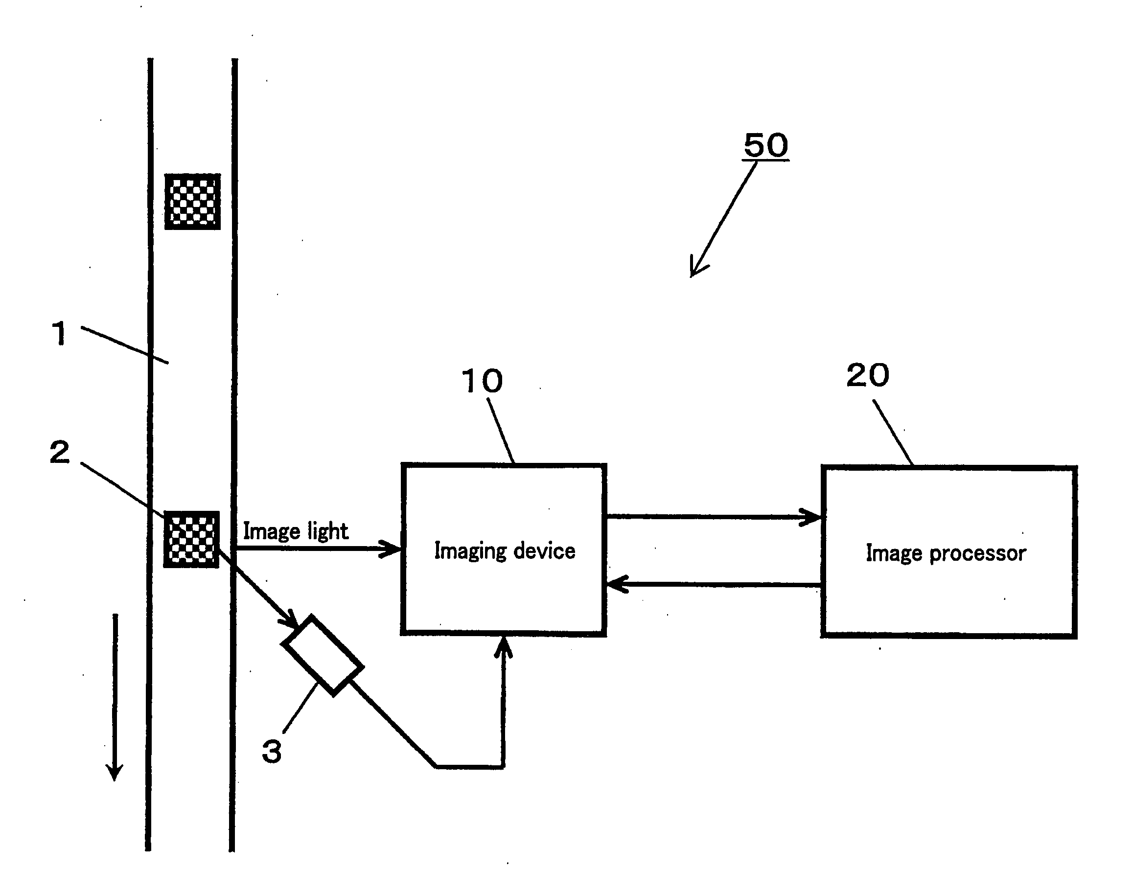
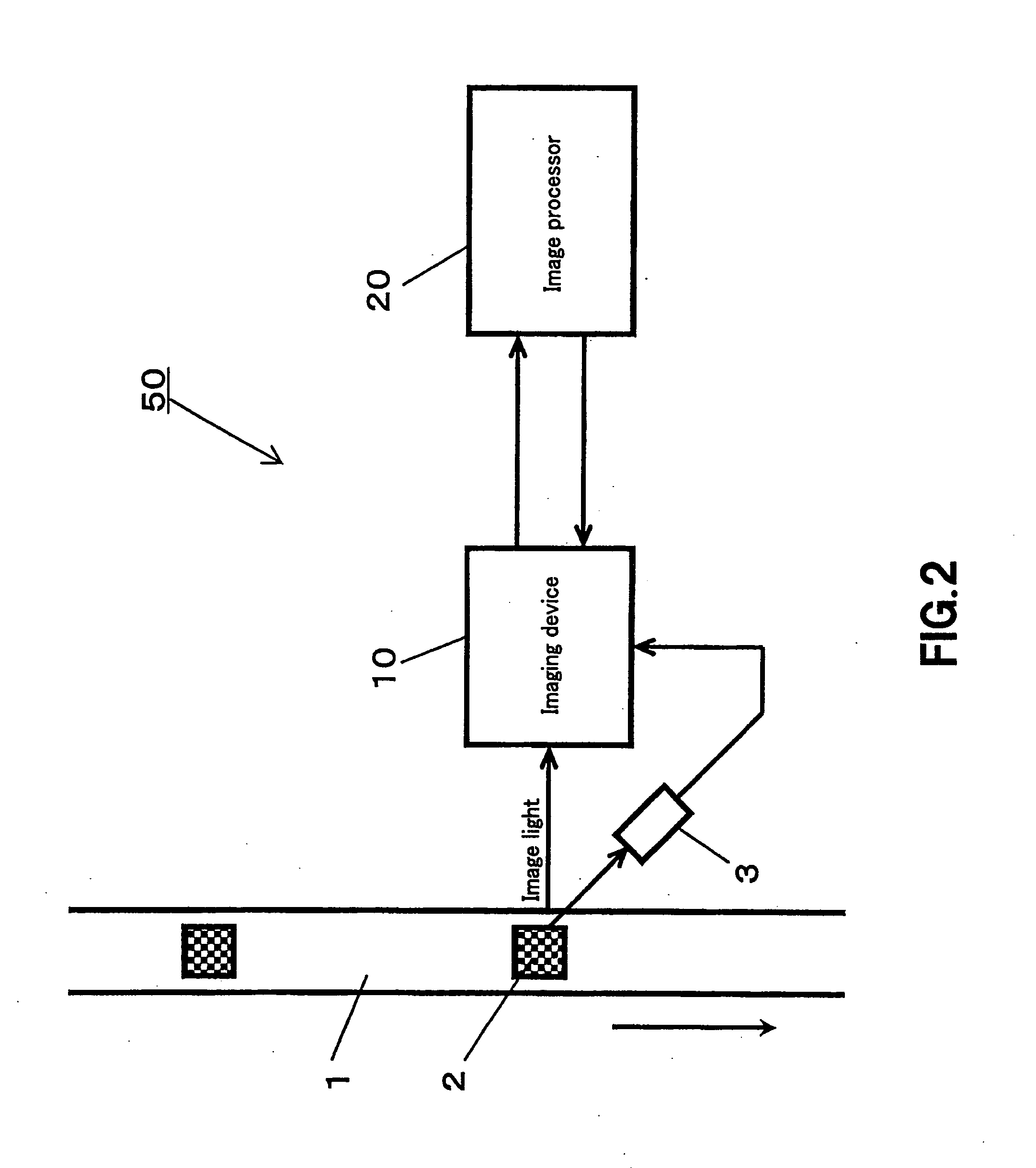
[0031] The present invention is applied to an imaging system, generally indicated with a reference numeral 50, constructed as schematically shown in FIG. 2.
[0032] In the imaging system 50, an object 2 being carried on a transfer path 1 such as a belt conveyor or the like is detected by an object sensor 3, it is imaged by an imaging device 10 on the basis of a detection output from the object sensor 3, and the captured image is taken in as a still picture. The image data captured by the imaging device 10 by imaging the object 2 on the basis of the detection output from the object sensor 3 is supplied to an image processor 20 also included in the imaging system 50.
[0033] In the imaging system 50, the object sensor 3 detects the object 2 being carried on the transfer path 1, a trigger signal TRIG is generated when the object 2 arrives at the front of the object sensor 3, and the trigger signal TRIG is supplied to the imaging device 10.
[0034] As shown in FIG. 3, the imaging device 10 includes a CCD image sensor 11, analog-digital converter 12 that digitizes an image signal (So) read from the CCD image sensor 11 and outputs it, memory 13 that provisionally saves the image signal (So) digitized by the analog-digital converter 12, and a timing generator 14 that gives an operation clock to each of the above other components of the imaging device 10.
[0035] The CCD image sensor 11 is of an interline transfer (IT) type constructed as shown in FIG. 4. It includes light-receiving elements SODD corresponding to pixels in odd fields and light-receiving elements SEVEN corresponding to pixels in even fields, vertical transfer units VREG to which charges stored in the light-receiving elements SODD and SEVEN are read, and a horizontal transfer unit HREG that outputs the charges read to the vertical transfer units HREG as image signals in units of one horizontal line. The CDD image sensor 11 performs an electronic shutter function by controlling the potential on a substrate (not shown) formed under the light-receiving elements SODD and SEVEN to sweep away the charges stored in the light-receiving elements SODD and SEVEN to the substrate in order to control the length of charge storage time.
[0036] The CCD image sensor 11 is driven the timing generator 13 to read the charges stored in the plurality of light-receiving elements SODD and SEVEN to the vertical transfer units VREG synchronously with the external trigger signal TRIG, transfer the charges read to the vertical transfer units VREG vertically at a first rate in response to a high-rate vertical transfer signal for the high-rate transfer period and transfer the charges in the vertical transfer units VREG vertically at a second rate slower than the first rate in response to a normal-rate vertical transfer signal for a normal-rate transfer period following the high-rate transfer period, to thereby output the charges supplied to the horizontal transfer unit HREG for the normal-rate transfer period as valid ones from the horizontal transfer unit HREG.
[0037] The timing generator 13 in the imaging device 10 has the substantial part thereof illustrated in FIG. 5. As shown, it includes a parameter setting block 131 to set parameters via a serial interface such as USB in response to a serial set signal supplied from the image processor 20, electronic shutter control signal generator 132 to generate an electronic shutter control signal corresponding to a parameter set in the parameter setting block, charge sweep-away signal switch 133 to select a path for a charge sweep-away signal output from the electronic shutter control signal generator 132, horizontal transfer signal generator 134 to generate a horizontal transfer signal corresponding to a parameter set in the parameter setting block 131, horizontal transfer signal switch 135 to select a path for a horizontal transfer signal output from the horizontal transfer signal generator 134, horizontal transfer signal generator 136 to generate a horizontal sync signal corresponding to a parameter set in the parameter setting block 131, horizontal sync signal switch 137 to select a path for a horizontal sync signal output from the horizontal transfer signal generator 136, vertical sync signal generator 138 to generate a vertical sync signal corresponding to a parameter set in the parameter setting block 131, vertical sync signal switch 139 to select a path for a vertical sync signal output from the vertical sync signal generator 138, etc.
[0038] The electronic shutter control signal generator 132 includes a normal-rate charge sweep-away signal generating block 132A to generate a normal-rate charge sweep-away signal SUB whose unit is a horizontal scanning period, fine-adjustment charge sweep-away signal generating block 132B to generate a fine-adjustment charge sweep-away signal SUB′ precisely corresponding to an arbitrary shutter speed fine-adjusted to an intended shutter speed such as 1/1000 sec or the like, and a sensor gate signal generating block 132C to generate a normal sensor gate signal SG.
[0039] Also, the horizontal transfer signal generator 134 includes a normal-rate charge horizontal transfer signal generating block 134A to generate a normal-rate horizontal transfer signal for a normal transfer rate corresponding to the normal-rate charge sweep-away signal SUB, and a fine-adjustment horizontal transfer signal generating block 134B to generate a fine-adjustment horizontal transfer signal corresponding to the fine-adjustment charge sweep-away signal SUB′.
[0040] Also, the horizontal sync signal generator 136 includes a normal-rate horizontal sync signal generating block 136A to generate a normal-rate horizontal sync signal and normal-rate horizontal blanking signal for a normal transfer rate corresponding to the normal-rate charge sweep-away signal SUB, and a fine-adjustment horizontal sync signal generating block 136B to generate a fine-adjustment horizontal sync signal and fine-adjustment horizontal blanking signal corresponding to the fine-adjustment charge sweep-away signal SUB′.
[0041] Further, the vertical sync signal generator 138 includes a normal-rate vertical sync signal generating block 138A to generate a normal-rate vertical sync signal and normal-rate vertical blanking signal for a normal transfer rate corresponding to the normal-rate charge sweep-away signal SUB, and a fine-adjustment vertical sync signal generating block 138B to generate a fine-adjustment vertical sync signal and fine-adjustment vertical blanking signal corresponding to the fine-adjustment charge sweep-away signal SUB′.
[0042] In the timing generator 13, when a trigger signal TRIG is supplied, the horizontal sync signal HD is reset while a vertical sync signal is generated, as shown in FIG. 6. Also, the shutter speed can be controlled in response to a width Wtrig.
[0043] Also, when supplied at the parameter setting block 131 with a shutter fine-adjustment command from the image processor 20 via the serial interface, the timing generator 13 changes the normal-rate charge sweep-away signal SUB whose unit is a signal horizontal scanning period, normal-rate horizontal transfer signal H1/H2/RQ normal-rate horizontal sync signal HD, normal-rate horizontal blanking signal HBLK, normal-rate vertical sync signal VD and normal-rate vertical blanking signal VBLK, generated by the normal-rate charge sweep-away signal generating block 132A, normal-rate horizontal transfer signal generating block 134A, normal-rate horizontal sync signal generating block 136A and normal-rate vertical sync signal generating block 138B, respectively, to the fine-adjustment charge sweep-away signal SUB′, fine-adjustment normal-rate horizontal transfer signal H1′/H2′/RQ fine-adjustment horizontal sync signal HD′, fine-adjustment horizontal blanking signal HBLK′, fine-adjustment vertical sync signal VD′ and fine-adjustment vertical blanking signal VBLK′, generated by the fine-adjustment charge sweep-away signal generating block 132B, fine-adjustment horizontal transfer signal generating block 134B, fine-adjustment horizontal sync signal generating block 136B and fine-adjustment vertical sync signal generating block 138B, respectively. Thus, the horizontal transfer signal H1/H2/RG supplied to the CCD image sensor 10 is stopped for a period for which the fine-adjustment charge sweep-away signal SUB′ occurs to make low the horizontal blanking signal HBLK′ low (an ineffective video period exists), and the effective video period is stopped once, as shown in FIG. 7. When the CCD image sensor 10 is driven, the invalid video part is increased simultaneously and also the period of a sync signal HD′/HBLK′/VD′/VBLK′ is increased.
[0044] With the above operations, the fine-adjustment charge sweep-away signal SUB′ is set in the ineffective video period and a video signal free of noise can be acquired with an accurate shutter speed.
[0045] With the above operations, the noise problem is solved, but the video signals cannot be acquired in succession. On this account, in the imaging device 10, horizontal transfer signals WRITE_HD/HBLK and READ_HD/HBLK generated by the horizontal transfer signal generator 136 in the timing generator 13 and vertical sync signals WRITE_VD/VBLK and READ_VD/VBLK generated by the vertical sync signal generator 138 are used to save the image signal (So) digitized by the analog-digital converter 12 provisionally in the memory 13, and the video signals are read continuously from the memory 13, as shown in FIG. 7.
[0046] It should be understood by those skilled in the art that various modifications, combinations, sub-combinations and alterations may occur depending on design requirements and other factors insofar as they are within the scope the appended claims or the equivalents thereof.

PUM

no PUM

Description & Claims & Application Information

We can also present the details of the Description, Claims and Application information to help users get a comprehensive understanding of the technical details of the patent, such as background art, summary of invention, brief description of drawings, description of embodiments, and other original content. On the other hand, users can also determine the specific scope of protection of the technology through the list of claims; as well as understand the changes in the life cycle of the technology with the presentation of the patent timeline. Login to view more.
Why Eureka
Try Eureka